www.techspot.com
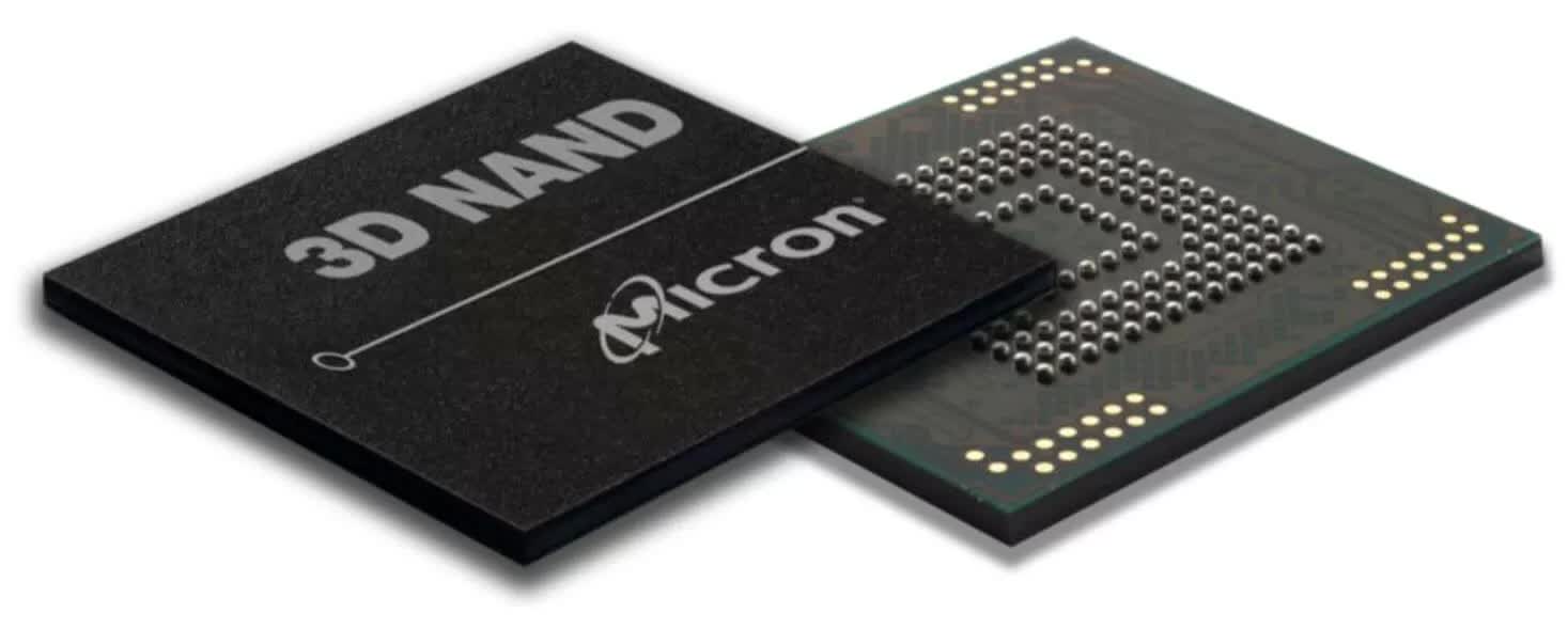
Freezing edge technology: A new plasma-based etching process could lead to denser data storage in phones, cameras, and computers. Researchers have developed a hydrogen fluoride plasma technique that doubles the etching rate in the manufacturing process of 3D NAND flash memory chips. Standard NAND flash storage is used in microSD cards, USB drives, and solid-state drives in computers and phones. To fit more gigabytes into smaller spaces, manufacturers have begun stacking memory cells vertically in a process called 3D NAND.Advancements in 3D NAND have pushed chip designs beyond 200 layers, with companies like Micron, SK Hynix, and Samsung already eyeing 400-layer technology to increase storage density. However, higher layer counts also bring greater manufacturing complexity. One particularly demanding process is etching, which requires meticulously carving precise holes, layer by layer, through alternating silicon oxide and silicon nitride layers.Researchers from Lam Research, the University of Colorado Boulder, and the Princeton Plasma Physics Laboratory (PPPL) have developed a new technique to streamline the process. It uses cryogenic (low-temperature) hydrogen fluoride plasma to etch the holes. In experiments, the etch rate more than doubled, increasing from 310 nanometers per minute with the old method to 640 nm/min with their approach. They also found that the etched holes were cleaner.Seeing benefits, the researchers experimented with adding a few other ingredients to the hydrogen fluoride plasma recipe. Phosphorus trifluoride acted as a nitrous boost for silicon dioxide etching, quadrupling the rate. They also tested ammonium fluorosilicate. The team detailed its findings in a study published in the Journal of Vacuum Science & Technology.Seeing benefits, the researchers explored adding a few other ingredients to this hydrogen fluoride plasma recipe. Phosphorus trifluoride acted as a nitrous boost for the silicon dioxide etching, quadrupling that rate. They also tested out ammonium fluorosilicate. The full findings can be found in the study published in the Journal of Vacuum Science & Technology. // Related StoriesWhile some challenges remain, the new technique could overcome a significant manufacturing hurdle. Igor Kaganovich, a principal research physicist at PPPL, pointed out that increasing memory density will be crucial as data demands grow with AI adoption.It's too early to say if this will result in cheaper or denser NAND chips for consumers. The technique still needs to be proven commercially viable and scaled for mass production. Even if manufacturers adopt the process, there's no guarantee that any cost savings will trickle down to consumers.