www.techspot.com
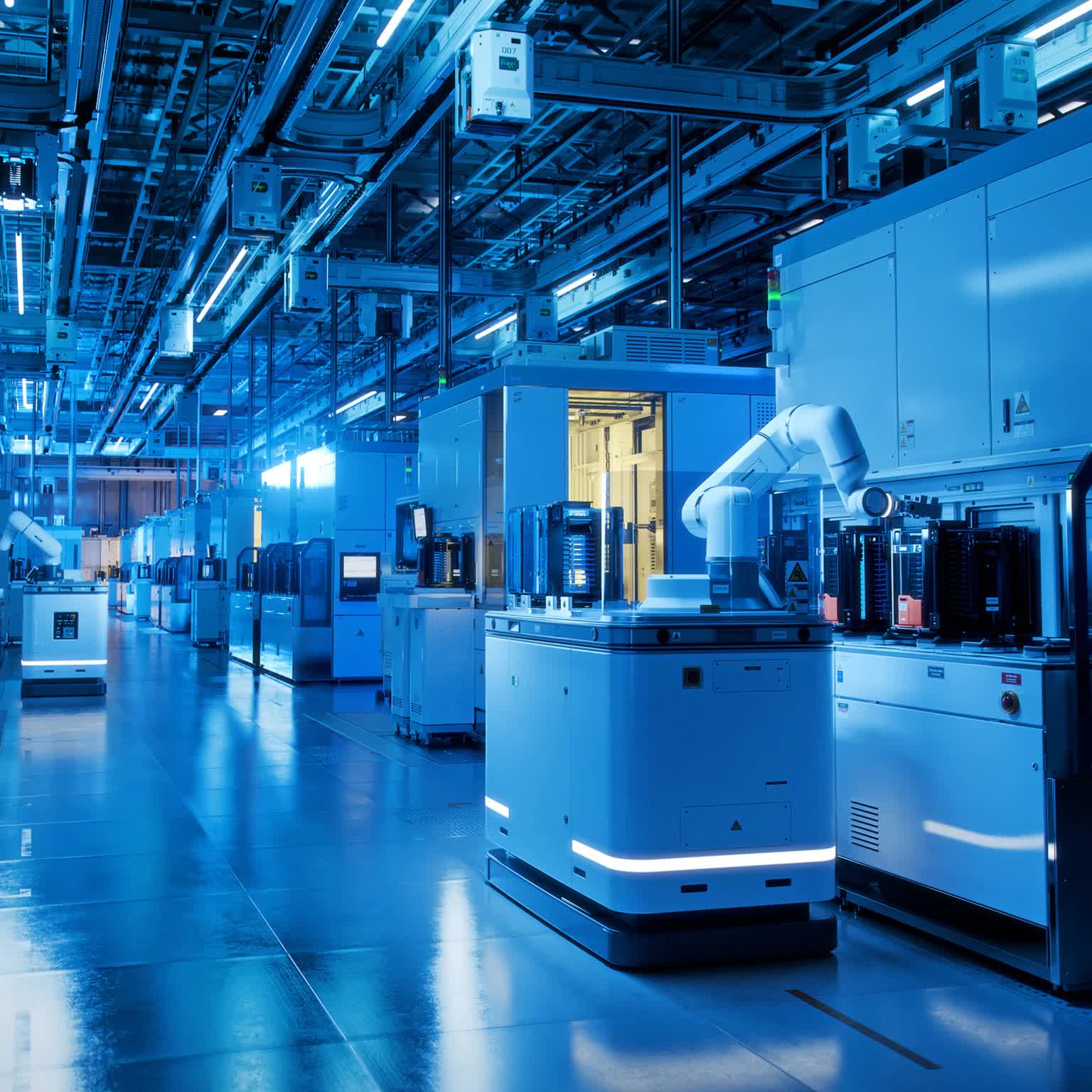
The big picture: The U.S. and many Western markets are simply not as efficient as Taiwan in building semiconductor fabrication (fab) operations. According to reports, 18 new fab construction projects are planned for 2025 alone, making it crucial to address these challenges. The West must streamline fab construction processes to catch up with the well-established semiconductor ecosystems of Taiwan and other Asian manufacturing hubs. TSMC encountered significant challenges when it began constructing its fab in Arizona, facing a trifecta of issues that underscored the stark contrast between fab construction in the U.S. and Taiwan. First, TSMC struggled to find skilled workers locally, a problem rarely encountered in Taiwan. Second, cultural differences between TSMC's Taiwanese management and American employees created unforeseen obstacles. Perhaps most critically, navigating local regulations proved difficult for the global chip manufacturer.However, these issues were not solely due to TSMC's inexperience in the U.S. market. Rather, they highlighted a fundamental gap in fab construction efficiency between the U.S. and Taiwan.Taiwan has developed remarkable expertise in building semiconductor fabrication facilities, closely followed by China and Southeast Asia. This efficiency is evident in the timelines and costs associated with fab construction across different regions.As reported by Semiconductor Digest, Herbert Blaschitz, Executive VP of the Global Business Unit for Advanced Technology Facilities at Exyte, spoke at the recent SEMI Industry Strategy Symposium and revealed that a very large fab in Taiwan owned by a U.S. company (which he declined to name) was built in approximately 20 months.In contrast, fabs in the U.S. typically take around 38 months to complete, from permitting and design to the start of wafer production. European fab construction falls between these extremes, averaging about 34 months.The cost disparity is equally striking. Construction costs for fabs in the U.S. are roughly double those in Taiwan, even though process equipment costs remain similar. Blaschitz succinctly summarized this difference: "Building a wafer fab in the West costs twice as much and takes twice the time compared to building one in Taiwan."The primary reason for Taiwan's superior efficiency in fab construction is experience. "Their supply chain is just unbelievably good," Blaschitz explained. "And very often, it's not that they are much more precise, but they know what they are doing." // Related StoriesThis experience translates into a more streamlined construction process. Taiwanese builders often work with less detailed information than their Western counterparts. "If you look at a drawing in Taiwan, half of the things that you would find in the Western world are missing," Blaschitz said. "They don't need that level of detail; they do it every day, and that makes them very productive."To fully grasp the magnitude of this efficiency gap, it is essential to understand the scale of modern fab construction. Today's semiconductor manufacturing facilities are marvels of engineering and logistics. According to Blaschitz, large fabs require over $20 billion in total capital expenditure, with $4-6 billion allocated solely to the facility itself.The construction of such a facility demands between 30 to 40 million work hours and involves managing vast quantities of materials, including 83,000 tons of steel reinforcement, 5,600 miles of cabling, and 785,000 cubic yards of concrete.A typical large-scale fab houses a 430,000-square-foot cleanroom containing 2,000 process tools. Each tool requires an average of 50 individual process and utility connections, resulting in over 50,000 total connections throughout the facility.The U.S. CHIPS Act aims to address this imbalance, but industry experts believe additional measures are necessary. Blaschitz advocates for "virtual commissioning" as a potential solution. This approach involves creating a digital twin of the fab during the planning and design phase, allowing for virtual commissioning before physical construction begins.