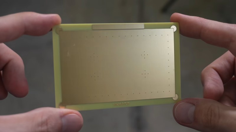
Samsung To Replace Silicon With Glass Interposers By 2028, Aiming For Faster AI Chips, Cheaper Manufacturing, And An Edge In Semiconductor Innovation
Samsung Electronics is taking a major step in the right direction in semiconductor innovation by planning to adopt glass substrate in chip packaging starting in 2028. If you are not familiar, the transition marks a major shift from silicon-based interposers to glass interposers, and it is the first time the company has laid out an official roadmap for the evolution, according to ETNews.
Samsung’s glass interposers could revolutionize AI chip packaging by offering better performance, lower costs, and faster production
In chip manufacturing, interposers are a key component in 2.5D chip packaging, especially for AI semiconductors, where the GPUs are surrounded by high-bandwidth memory or HBM. The interposers are responsible for connecting the two components, allowing for faster communication. While the traditional interposers are effective, they are quite expensive considering how the AI industry is on the rise. In comparison, the glass interposers are cheaper, but feature more precision for ultra-fine circuits and improved dimensional stability.
The benefits of the glass interposers definitely overtake the traditional interposers, which makes them a perfect option for next-gen AI chips. An industry official noted that “Samsung has established a plan to transition from silicon interposers to glass interposers in 2028 to meet customer demands.” The notion is in line with similar plans from competitors like AMD, which shows a surge in industry shift toward the new semiconductor technology.
While the industry is gradually embarking on the glass substrate bandwagon for interposers, Samsung's rendition of the technology is different, as it is developing sub-100x100mm glass units to speed up the prototyping instead of using large glass panels with a size of 510x515mm. Even though the smaller size could hurt the efficiency, it will allow the company to enter the market much faster.
Samsung is also utilizing its Cheonan campus panel-level packaging or PLP line, which makes use of square panels instead of round wafers. Overall, this will allow the company to sit in a much better position than the competition in the AI industry. Furthermore, the move also complements the company's AI Integrated Solution strategy, which would bring the foundry services, HBM memory, and advanced packaging under one umbrella.
With the AI industry booming rapidly, Samsung's transition to a glass substrate for interposers could give it an edge over the competition in the long run. Since the technology is going to improve gradually, the company could also benefit from external orders, which would allow it to increase its revenue. We will keep a close eye on the transition, so be sure to stick around for more details.
Deal of the Day
#samsung #replace #silicon #with #glass
·28 Views