


New research on 3D printing superconductors by Northwestern University
3dprintingindustry.com
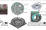
Researchers from Northwestern Universitys Department of Materials Science and Engineering and Fermi National Accelerator Laboratory have developed a way to 3D print single-crystal Yttrium barium copper oxide (YBCO) superconductors.Published in Nature Communications, their work addresses a major challenge in superconducting materials: how to retain the superior electrical properties of single-crystal structures while allowing for complex, functional designs.According to the researchers, superconductors like YBCO are already being used in MRI machines, nuclear magnetic resonance (NMR) systems, fusion energy projects, and maglev transportation. But they come with a tradeoff. The best-performing versions, those with a single-crystal structure, are brittle and difficult to shape beyond simple cylinders or blocks. On the other hand, polycrystalline versions, which can be 3D printed, have weak grain boundaries that limit their ability to carry current.Consequently, the team developed a two-step process that first prints the material as a polycrystalline structure and then converts it into a single crystal, maintaining both superconducting performance and design complexity.Schematic illustration of 3D-ink-extrusion printing, sintering, and top-seeded melt growth process of a toroidal Y123+Y211 coil. (PLGA: poly-lactic-co-glycolic-acid). The inset photograph shows a toroidal coil during layer-by-layer printing from bottom to top, using a 250m diameter nozzle. Image via Northwestern University.From polycrystalline to single-crystal precisionThe process begins with 3D printing a specialized ink containing yttrium oxide (YO), barium carbonate (BaCO), and copper oxide (CuO). Extruded through a 250 m nozzle, the ink forms detailed structures that gain strength as the solvent evaporates. A sintering process at 1000C for 20 hours then converts the material into a dense but polycrystalline YBCO superconductor.The next stage involves a critical modification. Introducing 69% yttrium barium copper oxide (Y123), 30% yttrium barium copper oxide (Y211, also known as the green phase), and 1% cerium oxide, the structure undergoes a second heat treatment, reaching 1090C. At this stage, a tiny neodymium barium copper oxide (NdBCO) seed crystal is placed on top. Cooling at a controlled rate of 0.5 Kelvin (K) per hour allows the material to reorganize into a single-crystal form, eliminating grain boundaries that previously hindered current flow.Testing revealed that the single-crystal version carried 66 times more electrical current than its polycrystalline counterpart at 77K, the temperature of liquid nitrogen. At 10K, current-carrying capacity increased 180 times. Operating temperature remained between 88 and 89.5K, slightly lower than the theoretical 93K due to trace impurities introduced during processing.A major concern when working with high-temperature superconductors is their tendency to collapse or deform during processing, especially when exposed to liquid phases at extreme heat.But the researchers discovered that YBaCuO (Y211) particles act as a built-in stabilizing framework, preventing slumping or sagging. This was backed by percolation theory, which explains how a network of solid particles can hold everything together even as other parts of the material liquefy.To demonstrate how practical this method could be, they 3D printed several complex superconducting structures, including levitating toroidal coils, magnetic shielding tubes, and origami-inspired designs. These would have been nearly impossible to manufacture using traditional single-crystal growth techniques. Their potential applications span particle accelerators, synchrotron undulators, and microwave cavities used in dark matter axion searches.Thats not to say the process is perfect just yet. The team observed minor defects, including small regions where crystal orientation misaligned, areas with localized porosity, and micro-cracks formed during oxygenation. If these cracks adversely impact mechanical and superconductivity properties, they can be mitigated by Ag additions, an approach to be explored in future research.As per the researchers, this research doesnt stop at superconductors. The same principles could apply to piezoelectric, thermoelectric, photovoltaic, and organic semiconductor materials, creating new possibilities in energy harvesting, electronics, and advanced materials development.3D printed poly- and monocrystalline objects with complex architectures. Image via Northwestern University.3D printing optimizes superconductor developmentNorthwestern University is the latest in a long list of superconductor research. Back in 2018, European Organization for Nuclear Research (CERN) chose Simufact Additive to enhance selective laser melting (SLM) 3D printing by predicting distortions and optimizing metal AM.The software provided simulation of laser powder bed fusion (PBF) processes, improving accuracy for superconducting magnets and RF components made from costly materials like niobium. In use for 15 months, Simufact also simulated heat treatment, support removal, and hot isostatic pressing (HIP) to mitigate residual stress and part failures.Professor Daniel Creedon from The University of Melbourne successfully demonstrated that 3D printing can produce superconducting microwave cavities with the same electrical properties as traditionally manufactured ones. These cavities, which store microwaves without energy loss, play a critical role in particle accelerators and precision measurement systems.Using SLM, Creedon fabricated two cavities from aluminum, one with 12% silicon, but found no significant difference in superconductivity. Both became active at 1.2K, though polishing and heat treatment at 770K doubled performance. At the time, these findings suggest 3D printed superconducting cavities could become viable for large-scale applications with further refinements.What3D printing trendsshould you watch out for in 2025?How is thefuture of 3D printingshaping up?To stay up to date with the latest 3D printing news, dont forget to subscribe to the 3D Printing Industry newsletter or follow us on Twitter, or like our page on Facebook.While youre here, why not subscribe to our Youtube channel? Featuring discussion, debriefs, video shorts, and webinar replays.Featured image shows schematic illustration of 3D-ink-extrusion printing, sintering, and top-seeded melt growth process of a toroidal Y123+Y211 coil. (PLGA: poly-lactic-co-glycolic-acid). The inset photograph shows a toroidal coil during layer-by-layer printing from bottom to top, using a 250m diameter nozzle. Image via Northwestern University.Ada ShaikhnagWith a background in journalism, Ada has a keen interest in frontier technology and its application in the wider world. Ada reports on aspects of 3D printing ranging from aerospace and automotive to medical and dental.
0 Commentaires
·0 Parts
·51 Vue