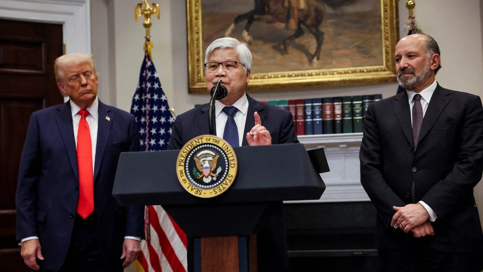
• Apple’s A20 Rumored To Be Exclusive To The iPhone 18 Pro, iPhone 18 Pro Max And The Company’s Foldable Flagship, Will Leverage TSMC’s Advanced 2nm Process Combined With The Newer WMCM Packaging

    Menu

    Home
    News

    Hardware

    Gaming

    Mobile

    Finance
    Deals
    Reviews
    How To

    Wccftech

    Apple’s A20 Rumored To Be Exclusive To The iPhone 18 Pro, iPhone 18 Pro Max And The Company’s Foldable Flagship, Will Leverage TSMC’s Advanced 2nm Process Combined With The Newer WMCM Packaging

    Omar Sohail •
    Jun 16, 2025 at 02:00am EDT

    TSMC might have started accepting orders for its 2nm wafers, but the first chipsets fabricated on this cutting-edge lithography are not expected to arrive until late next year. As the majority of you are well aware, Apple likely pounced on the opportunity to be the first recipient of this technology, with its A20 rumored to be mass produced on the 2nm process. However, the same rumor claims that the Cupertino firm will employ the foundry giant’s WMCMpackaging, bringing in more benefits, but customers can only experience these if they intend on making the iPhone 18 Pro, iPhone 18 Pro Max, or Apple’s upcoming foldable flagship their daily driver.
    The latest rumor also claims that Apple will not be upping the RAM count on any iPhone model that will ship with the A20
    The efforts to bring WMCM packaging to the A20 will be highly beneficial for Apple because it will allow the latter to maintain the chipset’s footprint while having immense flexibility in combining different components. In short, multiple dies such as the CPU, GPU, memory, and other parts can be integrated at a wafer level, before being sliced into individual chips. This approach will help Apple to mass manufacture smaller chipsets that are considerably power-efficient, but also powerful at the same time, leading to an incredible ‘performance per watt’ metric.
    China Times reports that this A20 upgrade will arrive for the iPhone 18 Pro, the iPhone 18 Pro Max, and Apple’s foldable flagship, which the rumor refers to as the iPhone 18 Fold. TSMC’s production line specifically for WMCM chipsets will be located in Chiayi AP7, with an estimated monthly production capacity of 50,000 pieces by the end of 2026. Interestingly, the RAM count will not change from this year, with Apple said to retain the 12GB limit. We have reported about the iPhone 18 series shifting to TSMC’s WMCM packaging before, while also talking about a separate rumor claiming that the A20 will be 15 percent faster than the A19 at the same power draw.
    The rumor does not mention whether the less expensive iPhone 18 models will be treated to chipsets featuring WMCM packaging, or if Apple intends to save on design and production costs by sticking with the older Integrated Fan-Outpackaging. All of these answers will be provided in the fourth quarter of 2026, when the iPhone 18 family goes official, so stay tuned.
    News Source: China Times

    Subscribe to get an everyday digest of the latest technology news in your inbox

    Follow us on

    Topics

    Sections

    Company

    Some posts on wccftech.com may contain affiliate links. We are a participant in the Amazon Services LLC
    Associates Program, an affiliate advertising program designed to provide a means for sites to earn
    advertising fees by advertising and linking to amazon.com
    © 2025 WCCF TECH INC. 700 - 401 West Georgia Street, Vancouver, BC, Canada
    #apples #a20 #rumored #exclusive #iphone
    Apple’s A20 Rumored To Be Exclusive To The iPhone 18 Pro, iPhone 18 Pro Max And The Company’s Foldable Flagship, Will Leverage TSMC’s Advanced 2nm Process Combined With The Newer WMCM Packaging
    Menu Home News Hardware Gaming Mobile Finance Deals Reviews How To Wccftech Apple’s A20 Rumored To Be Exclusive To The iPhone 18 Pro, iPhone 18 Pro Max And The Company’s Foldable Flagship, Will Leverage TSMC’s Advanced 2nm Process Combined With The Newer WMCM Packaging Omar Sohail • Jun 16, 2025 at 02:00am EDT TSMC might have started accepting orders for its 2nm wafers, but the first chipsets fabricated on this cutting-edge lithography are not expected to arrive until late next year. As the majority of you are well aware, Apple likely pounced on the opportunity to be the first recipient of this technology, with its A20 rumored to be mass produced on the 2nm process. However, the same rumor claims that the Cupertino firm will employ the foundry giant’s WMCMpackaging, bringing in more benefits, but customers can only experience these if they intend on making the iPhone 18 Pro, iPhone 18 Pro Max, or Apple’s upcoming foldable flagship their daily driver. The latest rumor also claims that Apple will not be upping the RAM count on any iPhone model that will ship with the A20 The efforts to bring WMCM packaging to the A20 will be highly beneficial for Apple because it will allow the latter to maintain the chipset’s footprint while having immense flexibility in combining different components. In short, multiple dies such as the CPU, GPU, memory, and other parts can be integrated at a wafer level, before being sliced into individual chips. This approach will help Apple to mass manufacture smaller chipsets that are considerably power-efficient, but also powerful at the same time, leading to an incredible ‘performance per watt’ metric. China Times reports that this A20 upgrade will arrive for the iPhone 18 Pro, the iPhone 18 Pro Max, and Apple’s foldable flagship, which the rumor refers to as the iPhone 18 Fold. TSMC’s production line specifically for WMCM chipsets will be located in Chiayi AP7, with an estimated monthly production capacity of 50,000 pieces by the end of 2026. Interestingly, the RAM count will not change from this year, with Apple said to retain the 12GB limit. We have reported about the iPhone 18 series shifting to TSMC’s WMCM packaging before, while also talking about a separate rumor claiming that the A20 will be 15 percent faster than the A19 at the same power draw. The rumor does not mention whether the less expensive iPhone 18 models will be treated to chipsets featuring WMCM packaging, or if Apple intends to save on design and production costs by sticking with the older Integrated Fan-Outpackaging. All of these answers will be provided in the fourth quarter of 2026, when the iPhone 18 family goes official, so stay tuned. News Source: China Times Subscribe to get an everyday digest of the latest technology news in your inbox Follow us on Topics Sections Company Some posts on wccftech.com may contain affiliate links. We are a participant in the Amazon Services LLC Associates Program, an affiliate advertising program designed to provide a means for sites to earn advertising fees by advertising and linking to amazon.com © 2025 WCCF TECH INC. 700 - 401 West Georgia Street, Vancouver, BC, Canada #apples #a20 #rumored #exclusive #iphone
    WCCFTECH.COM
    Apple’s A20 Rumored To Be Exclusive To The iPhone 18 Pro, iPhone 18 Pro Max And The Company’s Foldable Flagship, Will Leverage TSMC’s Advanced 2nm Process Combined With The Newer WMCM Packaging
    Menu Home News Hardware Gaming Mobile Finance Deals Reviews How To Wccftech Apple’s A20 Rumored To Be Exclusive To The iPhone 18 Pro, iPhone 18 Pro Max And The Company’s Foldable Flagship, Will Leverage TSMC’s Advanced 2nm Process Combined With The Newer WMCM Packaging Omar Sohail • Jun 16, 2025 at 02:00am EDT TSMC might have started accepting orders for its 2nm wafers, but the first chipsets fabricated on this cutting-edge lithography are not expected to arrive until late next year. As the majority of you are well aware, Apple likely pounced on the opportunity to be the first recipient of this technology, with its A20 rumored to be mass produced on the 2nm process. However, the same rumor claims that the Cupertino firm will employ the foundry giant’s WMCM (Wafer-Level Multi-Chip Module) packaging, bringing in more benefits, but customers can only experience these if they intend on making the iPhone 18 Pro, iPhone 18 Pro Max, or Apple’s upcoming foldable flagship their daily driver. The latest rumor also claims that Apple will not be upping the RAM count on any iPhone model that will ship with the A20 The efforts to bring WMCM packaging to the A20 will be highly beneficial for Apple because it will allow the latter to maintain the chipset’s footprint while having immense flexibility in combining different components. In short, multiple dies such as the CPU, GPU, memory, and other parts can be integrated at a wafer level, before being sliced into individual chips. This approach will help Apple to mass manufacture smaller chipsets that are considerably power-efficient, but also powerful at the same time, leading to an incredible ‘performance per watt’ metric. China Times reports that this A20 upgrade will arrive for the iPhone 18 Pro, the iPhone 18 Pro Max, and Apple’s foldable flagship, which the rumor refers to as the iPhone 18 Fold. TSMC’s production line specifically for WMCM chipsets will be located in Chiayi AP7, with an estimated monthly production capacity of 50,000 pieces by the end of 2026. Interestingly, the RAM count will not change from this year, with Apple said to retain the 12GB limit. We have reported about the iPhone 18 series shifting to TSMC’s WMCM packaging before, while also talking about a separate rumor claiming that the A20 will be 15 percent faster than the A19 at the same power draw. The rumor does not mention whether the less expensive iPhone 18 models will be treated to chipsets featuring WMCM packaging, or if Apple intends to save on design and production costs by sticking with the older Integrated Fan-Out (InFo) packaging. All of these answers will be provided in the fourth quarter of 2026, when the iPhone 18 family goes official, so stay tuned. News Source: China Times Subscribe to get an everyday digest of the latest technology news in your inbox Follow us on Topics Sections Company Some posts on wccftech.com may contain affiliate links. We are a participant in the Amazon Services LLC Associates Program, an affiliate advertising program designed to provide a means for sites to earn advertising fees by advertising and linking to amazon.com © 2025 WCCF TECH INC. 700 - 401 West Georgia Street, Vancouver, BC, Canada
    Like
    Love
    Wow
    Angry
    Sad
    470
    2 Comments 0 Shares
  • Apple is reportedly redesigning the MacBook Pro next year, here’s what we’re expecting

    Rumors strongly suggest that Apple will be overhauling the MacBook Pro in 2026, marking five years since the previous redesign that we know and love today. There are three key rumors to follow with this redesigned MacBook Pro, and we’ll be delving into them here.

    OLED display
    After debuting in the iPad Pro in 2024, Apple is expected to introduce OLED display technology to the MacBook Pro for the very first time with the redesign in 2026. This’ll provide higher brightness, better contrast ratios, and nicer colors to the MacBook Pro lineup for the very first time.
    Plus, according to TheElec, Apple will be using the same Tandem OLED display tech as the aforementioned iPad Pro:

    The OLED MacBook Air is also expected to get a standard single-stack display, rather than the more sophisticated Two-Stack Tandem displays we reported on for the MacBook Pro.
    Single-stack displays have one red, green and blue layer, while two-stack tandem OLED has a second RGB layer. Two layers stacked in tandem increases the brightness of the screen, while also increasing longevity.

    While transitioning to OLED, Apple may also ditch the notch, in favor of a smaller camera hole cutout. This information comes from Omdia, who describes it as a “rounded corner + hole cut.”
    The report doesn’t specify whether or not it’ll be a single hole punch, or something more similar to Dynamic Island on the iPhone. Either way, there won’t be as chunky of a cutout in your MacBook Pro display once the redesign arrives.
    Thinner design
    According to Bloomberg, Apple will be adopting a new, thinner design with the 2026 MacBook Pro. There aren’t many other details specified, so it’s unclear if the overall chassis design will change:

    Though Apple has continued to enhance the product with new chips and other internal improvements, the MacBook Pro probably won’t get another true overhaul until 2026. The company had once hoped to release this new version in 2025 — with a thinner design and a move to crisper OLED screens — but there were delays related to the display technology.

    Cutting-edge M6 chip
    Apple will also debut the M6 family of chips in this new MacBook Pro redesign. Currently, M6 is anticipated to be the first generation of Apple Silicon to adopt TSMC’s 2nm technology, alongside the A20 chip for iPhone.
    As per usual, we should see M6, M6 Pro, and M6 Max versions of the MacBook Pro, in both 14-inch and 16-inch sizes. With a new process node, we should see noticeable performance and efficiency gains.
    Wrap up
    Overall, the biggest feature of this upgrade is certainly the fact that the MacBook Pro will be adopting OLED. That said, I’ll certainly appreciate the thinner design – particularly on the 16-inch MacBook Pro, which currently comes in at 4.7 pounds.
    In case you aren’t too fond of waiting around a year and a half to buy a new MacBook Pro, there are some good discounts on the current M4 MacBook Pro models now that they’re around halfway through their lifespan. You can pick up an M4 14-inch for an M4 Pro 14-inch for or an M4 Pro 16-inch for These are all around off compared to their typical prices.

    My favorite Apple accessory recommendations:
    Follow Michael: X/Twitter, Bluesky, Instagram

    Add 9to5Mac to your Google News feed. 

    FTC: We use income earning auto affiliate links. More.You’re reading 9to5Mac — experts who break news about Apple and its surrounding ecosystem, day after day. Be sure to check out our homepage for all the latest news, and follow 9to5Mac on Twitter, Facebook, and LinkedIn to stay in the loop. Don’t know where to start? Check out our exclusive stories, reviews, how-tos, and subscribe to our YouTube channel
    #apple #reportedly #redesigning #macbook #pro
    Apple is reportedly redesigning the MacBook Pro next year, here’s what we’re expecting
    Rumors strongly suggest that Apple will be overhauling the MacBook Pro in 2026, marking five years since the previous redesign that we know and love today. There are three key rumors to follow with this redesigned MacBook Pro, and we’ll be delving into them here. OLED display After debuting in the iPad Pro in 2024, Apple is expected to introduce OLED display technology to the MacBook Pro for the very first time with the redesign in 2026. This’ll provide higher brightness, better contrast ratios, and nicer colors to the MacBook Pro lineup for the very first time. Plus, according to TheElec, Apple will be using the same Tandem OLED display tech as the aforementioned iPad Pro: The OLED MacBook Air is also expected to get a standard single-stack display, rather than the more sophisticated Two-Stack Tandem displays we reported on for the MacBook Pro. Single-stack displays have one red, green and blue layer, while two-stack tandem OLED has a second RGB layer. Two layers stacked in tandem increases the brightness of the screen, while also increasing longevity. While transitioning to OLED, Apple may also ditch the notch, in favor of a smaller camera hole cutout. This information comes from Omdia, who describes it as a “rounded corner + hole cut.” The report doesn’t specify whether or not it’ll be a single hole punch, or something more similar to Dynamic Island on the iPhone. Either way, there won’t be as chunky of a cutout in your MacBook Pro display once the redesign arrives. Thinner design According to Bloomberg, Apple will be adopting a new, thinner design with the 2026 MacBook Pro. There aren’t many other details specified, so it’s unclear if the overall chassis design will change: Though Apple has continued to enhance the product with new chips and other internal improvements, the MacBook Pro probably won’t get another true overhaul until 2026. The company had once hoped to release this new version in 2025 — with a thinner design and a move to crisper OLED screens — but there were delays related to the display technology. Cutting-edge M6 chip Apple will also debut the M6 family of chips in this new MacBook Pro redesign. Currently, M6 is anticipated to be the first generation of Apple Silicon to adopt TSMC’s 2nm technology, alongside the A20 chip for iPhone. As per usual, we should see M6, M6 Pro, and M6 Max versions of the MacBook Pro, in both 14-inch and 16-inch sizes. With a new process node, we should see noticeable performance and efficiency gains. Wrap up Overall, the biggest feature of this upgrade is certainly the fact that the MacBook Pro will be adopting OLED. That said, I’ll certainly appreciate the thinner design – particularly on the 16-inch MacBook Pro, which currently comes in at 4.7 pounds. In case you aren’t too fond of waiting around a year and a half to buy a new MacBook Pro, there are some good discounts on the current M4 MacBook Pro models now that they’re around halfway through their lifespan. You can pick up an M4 14-inch for an M4 Pro 14-inch for or an M4 Pro 16-inch for These are all around off compared to their typical prices. My favorite Apple accessory recommendations: Follow Michael: X/Twitter, Bluesky, Instagram Add 9to5Mac to your Google News feed.  FTC: We use income earning auto affiliate links. More.You’re reading 9to5Mac — experts who break news about Apple and its surrounding ecosystem, day after day. Be sure to check out our homepage for all the latest news, and follow 9to5Mac on Twitter, Facebook, and LinkedIn to stay in the loop. Don’t know where to start? Check out our exclusive stories, reviews, how-tos, and subscribe to our YouTube channel #apple #reportedly #redesigning #macbook #pro
    9TO5MAC.COM
    Apple is reportedly redesigning the MacBook Pro next year, here’s what we’re expecting
    Rumors strongly suggest that Apple will be overhauling the MacBook Pro in 2026, marking five years since the previous redesign that we know and love today. There are three key rumors to follow with this redesigned MacBook Pro, and we’ll be delving into them here. OLED display After debuting in the iPad Pro in 2024, Apple is expected to introduce OLED display technology to the MacBook Pro for the very first time with the redesign in 2026. This’ll provide higher brightness, better contrast ratios, and nicer colors to the MacBook Pro lineup for the very first time. Plus, according to TheElec, Apple will be using the same Tandem OLED display tech as the aforementioned iPad Pro: The OLED MacBook Air is also expected to get a standard single-stack display, rather than the more sophisticated Two-Stack Tandem displays we reported on for the MacBook Pro. Single-stack displays have one red, green and blue layer, while two-stack tandem OLED has a second RGB layer. Two layers stacked in tandem increases the brightness of the screen, while also increasing longevity. While transitioning to OLED, Apple may also ditch the notch, in favor of a smaller camera hole cutout. This information comes from Omdia, who describes it as a “rounded corner + hole cut.” The report doesn’t specify whether or not it’ll be a single hole punch, or something more similar to Dynamic Island on the iPhone. Either way, there won’t be as chunky of a cutout in your MacBook Pro display once the redesign arrives. Thinner design According to Bloomberg, Apple will be adopting a new, thinner design with the 2026 MacBook Pro. There aren’t many other details specified, so it’s unclear if the overall chassis design will change: Though Apple has continued to enhance the product with new chips and other internal improvements, the MacBook Pro probably won’t get another true overhaul until 2026. The company had once hoped to release this new version in 2025 — with a thinner design and a move to crisper OLED screens — but there were delays related to the display technology. Cutting-edge M6 chip Apple will also debut the M6 family of chips in this new MacBook Pro redesign. Currently, M6 is anticipated to be the first generation of Apple Silicon to adopt TSMC’s 2nm technology, alongside the A20 chip for iPhone. As per usual, we should see M6, M6 Pro, and M6 Max versions of the MacBook Pro, in both 14-inch and 16-inch sizes. With a new process node, we should see noticeable performance and efficiency gains. Wrap up Overall, the biggest feature of this upgrade is certainly the fact that the MacBook Pro will be adopting OLED. That said, I’ll certainly appreciate the thinner design – particularly on the 16-inch MacBook Pro, which currently comes in at 4.7 pounds. In case you aren’t too fond of waiting around a year and a half to buy a new MacBook Pro, there are some good discounts on the current M4 MacBook Pro models now that they’re around halfway through their lifespan. You can pick up an M4 14-inch for $1429, an M4 Pro 14-inch for $1779, or an M4 Pro 16-inch for $2249. These are all around $200 off compared to their typical prices. My favorite Apple accessory recommendations: Follow Michael: X/Twitter, Bluesky, Instagram Add 9to5Mac to your Google News feed.  FTC: We use income earning auto affiliate links. More.You’re reading 9to5Mac — experts who break news about Apple and its surrounding ecosystem, day after day. Be sure to check out our homepage for all the latest news, and follow 9to5Mac on Twitter, Facebook, and LinkedIn to stay in the loop. Don’t know where to start? Check out our exclusive stories, reviews, how-tos, and subscribe to our YouTube channel
    0 Comments 0 Shares
  • Xiaomi Cannot Develop A Future In-House XRING Chipset Using TSMC’s 2nm Process Because Of The U.S. Crackdown On Specialized EDA Tools, Company Will Be Limited To The ‘N3E’ Node

    Menu

    Home
    News

    Hardware

    Gaming

    Mobile

    Finance
    Deals
    Reviews
    How To

    Wccftech

    Xiaomi Cannot Develop A Future In-House XRING Chipset Using TSMC’s 2nm Process Because Of The U.S. Crackdown On Specialized EDA Tools, Company Will Be Limited To The ‘N3E’ Node

    Omar Sohail •
    Jun 5, 2025 at 04:28am EDT

    The XRING 01 is a technological milestone, not just for Xiaomi, but it is also regarded as an achievement for China, and one that would make the U.S. government very nervous, because, like current-generation chipsets, the in-house solution has been mass produced on TSMC’s 3nm ‘N3E’ process. Unfortunately, Xiaomi’s progress might not scale past this threshold because the Trump administration has banned the export of EDA tools that are necessary to successfully fabricate a 2nm SoC.
    Tipster claims that EDA tools are mandatory in designing GAAFET structures, meaning that Xiaomi and its XRING division will be limited to TSMC’s ‘N3E’ node
    Since TSMC’s 2nm technology has a GAAFET structure, Weibo tipster Digital Chat Station states that it is imperative that Xiaomi gets hold of those EDA, or Electronic Design Automation tools. The Taiwanese semiconductor giant was reported to have begun accepting orders for 2nm wafers from April 1, with each unit estimated to cost Among the regular trio of Apple, Qualcomm, and MediaTek, Xiaomi would count itself as one of TSMC’s customers. Sadly, with the recent development, the Chinese firm will be limited to the 3nm N3E node, facing a similar fate to Huawei.
    The latest claim also suggests that to possess the latest and greatest hardware in smartphone chipset technology, Xiaomi will have little choice but to continue relying on Qualcomm and MediaTek, which will unveil the Snapdragon 8 Elite Gen 2 and Dimensity 9500 later this year. Fortunately, restricting exports of cutting-edge machinery to China will only boost its resolve to continue the production of local EDA tools, but will this hardware be developed fast enough for the Xiaomi XRING 02 to be fabricated on TSMC’s 2nm process? We will have the answer to this question in the future.

    Readers should note that there is also the risk that the Trump administration enforces a massive ban on Xiaomi, preventing the latter from doing business with TSMC or Samsung in any way, shape, or form. While China is pursuing the manufacturing of custom EUV machinery to eliminate any overseas trade involvement, it may take several years for the country to achieve autonomy.
    News Source: Digital Chat Station

    Subscribe to get an everyday digest of the latest technology news in your inbox

    Follow us on

    Topics

    Sections

    Company

    Some posts on wccftech.com may contain affiliate links. We are a participant in the Amazon Services LLC
    Associates Program, an affiliate advertising program designed to provide a means for sites to earn
    advertising fees by advertising and linking to amazon.com
    © 2025 WCCF TECH INC. 700 - 401 West Georgia Street, Vancouver, BC, Canada
    #xiaomi #cannot #develop #future #inhouse
    Xiaomi Cannot Develop A Future In-House XRING Chipset Using TSMC’s 2nm Process Because Of The U.S. Crackdown On Specialized EDA Tools, Company Will Be Limited To The ‘N3E’ Node
    Menu Home News Hardware Gaming Mobile Finance Deals Reviews How To Wccftech Xiaomi Cannot Develop A Future In-House XRING Chipset Using TSMC’s 2nm Process Because Of The U.S. Crackdown On Specialized EDA Tools, Company Will Be Limited To The ‘N3E’ Node Omar Sohail • Jun 5, 2025 at 04:28am EDT The XRING 01 is a technological milestone, not just for Xiaomi, but it is also regarded as an achievement for China, and one that would make the U.S. government very nervous, because, like current-generation chipsets, the in-house solution has been mass produced on TSMC’s 3nm ‘N3E’ process. Unfortunately, Xiaomi’s progress might not scale past this threshold because the Trump administration has banned the export of EDA tools that are necessary to successfully fabricate a 2nm SoC. Tipster claims that EDA tools are mandatory in designing GAAFET structures, meaning that Xiaomi and its XRING division will be limited to TSMC’s ‘N3E’ node Since TSMC’s 2nm technology has a GAAFET structure, Weibo tipster Digital Chat Station states that it is imperative that Xiaomi gets hold of those EDA, or Electronic Design Automation tools. The Taiwanese semiconductor giant was reported to have begun accepting orders for 2nm wafers from April 1, with each unit estimated to cost Among the regular trio of Apple, Qualcomm, and MediaTek, Xiaomi would count itself as one of TSMC’s customers. Sadly, with the recent development, the Chinese firm will be limited to the 3nm N3E node, facing a similar fate to Huawei. The latest claim also suggests that to possess the latest and greatest hardware in smartphone chipset technology, Xiaomi will have little choice but to continue relying on Qualcomm and MediaTek, which will unveil the Snapdragon 8 Elite Gen 2 and Dimensity 9500 later this year. Fortunately, restricting exports of cutting-edge machinery to China will only boost its resolve to continue the production of local EDA tools, but will this hardware be developed fast enough for the Xiaomi XRING 02 to be fabricated on TSMC’s 2nm process? We will have the answer to this question in the future. Readers should note that there is also the risk that the Trump administration enforces a massive ban on Xiaomi, preventing the latter from doing business with TSMC or Samsung in any way, shape, or form. While China is pursuing the manufacturing of custom EUV machinery to eliminate any overseas trade involvement, it may take several years for the country to achieve autonomy. News Source: Digital Chat Station Subscribe to get an everyday digest of the latest technology news in your inbox Follow us on Topics Sections Company Some posts on wccftech.com may contain affiliate links. We are a participant in the Amazon Services LLC Associates Program, an affiliate advertising program designed to provide a means for sites to earn advertising fees by advertising and linking to amazon.com © 2025 WCCF TECH INC. 700 - 401 West Georgia Street, Vancouver, BC, Canada #xiaomi #cannot #develop #future #inhouse
    WCCFTECH.COM
    Xiaomi Cannot Develop A Future In-House XRING Chipset Using TSMC’s 2nm Process Because Of The U.S. Crackdown On Specialized EDA Tools, Company Will Be Limited To The ‘N3E’ Node
    Menu Home News Hardware Gaming Mobile Finance Deals Reviews How To Wccftech Xiaomi Cannot Develop A Future In-House XRING Chipset Using TSMC’s 2nm Process Because Of The U.S. Crackdown On Specialized EDA Tools, Company Will Be Limited To The ‘N3E’ Node Omar Sohail • Jun 5, 2025 at 04:28am EDT The XRING 01 is a technological milestone, not just for Xiaomi, but it is also regarded as an achievement for China, and one that would make the U.S. government very nervous, because, like current-generation chipsets, the in-house solution has been mass produced on TSMC’s 3nm ‘N3E’ process. Unfortunately, Xiaomi’s progress might not scale past this threshold because the Trump administration has banned the export of EDA tools that are necessary to successfully fabricate a 2nm SoC. Tipster claims that EDA tools are mandatory in designing GAAFET structures, meaning that Xiaomi and its XRING division will be limited to TSMC’s ‘N3E’ node Since TSMC’s 2nm technology has a GAAFET structure, Weibo tipster Digital Chat Station states that it is imperative that Xiaomi gets hold of those EDA, or Electronic Design Automation tools. The Taiwanese semiconductor giant was reported to have begun accepting orders for 2nm wafers from April 1, with each unit estimated to cost $30,000. Among the regular trio of Apple, Qualcomm, and MediaTek, Xiaomi would count itself as one of TSMC’s customers. Sadly, with the recent development, the Chinese firm will be limited to the 3nm N3E node, facing a similar fate to Huawei. The latest claim also suggests that to possess the latest and greatest hardware in smartphone chipset technology, Xiaomi will have little choice but to continue relying on Qualcomm and MediaTek, which will unveil the Snapdragon 8 Elite Gen 2 and Dimensity 9500 later this year. Fortunately, restricting exports of cutting-edge machinery to China will only boost its resolve to continue the production of local EDA tools, but will this hardware be developed fast enough for the Xiaomi XRING 02 to be fabricated on TSMC’s 2nm process? We will have the answer to this question in the future. Readers should note that there is also the risk that the Trump administration enforces a massive ban on Xiaomi, preventing the latter from doing business with TSMC or Samsung in any way, shape, or form. While China is pursuing the manufacturing of custom EUV machinery to eliminate any overseas trade involvement, it may take several years for the country to achieve autonomy. News Source: Digital Chat Station Subscribe to get an everyday digest of the latest technology news in your inbox Follow us on Topics Sections Company Some posts on wccftech.com may contain affiliate links. We are a participant in the Amazon Services LLC Associates Program, an affiliate advertising program designed to provide a means for sites to earn advertising fees by advertising and linking to amazon.com © 2025 WCCF TECH INC. 700 - 401 West Georgia Street, Vancouver, BC, Canada
    Like
    Love
    Wow
    Sad
    Angry
    325
    0 Comments 0 Shares
  • TSMC's 2nm wafer prices hit $30,000 as SRAM yields reportedly hit 90%

    In context: TSMC has steadily raised the prices of its most advanced semiconductor process nodes over the past several years – so much so that one analysis suggests the cost per transistor hasn't decreased in over a decade. Further price hikes, driven by tariffs and rising development costs, are reinforcing the notion that Moore's Law is truly dead.
    The Commercial Times reports that TSMC's upcoming N2 2nm semiconductors will cost per wafer, a roughly 66% increase over the company's 3nm chips. Future nodes are expected to be even more expensive and likely reserved for the largest manufacturers.
    TSMC has justified these price increases by citing the massive cost of building 2nm fabrication plants, which can reach up to million. According to United Daily News, major players such as Apple, AMD, Qualcomm, Broadcom, and Nvidia are expected to place orders before the end of the year despite the higher prices, potentially bringing TSMC's 2nm Arizona fab to full capacity.
    Also see: How profitable are TSMC's nodes: crunching the numbers
    Unsurprisingly, Apple is getting first dibs. The A20 processor in next year's iPhone 18 Pro is expected to be the first chip based on TSMC's N2 process. Intel's Nova Lake processors, targeting desktops and possibly high-end laptops, are also slated to use N2 and are expected to launch next year.
    Earlier reports indicated that yield rates for TSMC's 2nm process reached 60% last year and have since improved. New data suggests that 256Mb SRAM yield rates now exceed 90%. Trial production is likely already underway, with mass production scheduled to begin later this year.
    // Related Stories

    With tape-outs for 2nm-based designs surpassing previous nodes at the same development stage, TSMC aims to produce tens of thousands of wafers by the end of 2025.

    TSMC also plans to follow N2 with N2P and N2X in the second half of next year. N2P is expected to offer an 18% performance boost over N3E at the same power level and 36% greater energy efficiency at the same speed, along with significantly higher logic density. N2X, slated for mass production in 2027, will increase maximum clock frequencies by 10%.
    As semiconductor geometries continue to shrink, power leakage becomes a major concern. TSMC's 2nm nodes will address this issue with gate-all-aroundtransistor architectures, enabling more precise control of electrical currents.
    Beyond 2nm lies the Angstrom era, where TSMC will implement backside power delivery to further enhance performance. Future process nodes like A16and A14could cost up to per wafer.
    Meanwhile, Intel is aiming to outpace TSMC's roadmap. The company recently began risk production of its A18 node, which also features gate-all-around and backside power delivery. These chips are expected to debut later this year in Intel's upcoming laptop CPUs, codenamed Panther Lake.
    #tsmc039s #2nm #wafer #prices #hit
    TSMC's 2nm wafer prices hit $30,000 as SRAM yields reportedly hit 90%
    In context: TSMC has steadily raised the prices of its most advanced semiconductor process nodes over the past several years – so much so that one analysis suggests the cost per transistor hasn't decreased in over a decade. Further price hikes, driven by tariffs and rising development costs, are reinforcing the notion that Moore's Law is truly dead. The Commercial Times reports that TSMC's upcoming N2 2nm semiconductors will cost per wafer, a roughly 66% increase over the company's 3nm chips. Future nodes are expected to be even more expensive and likely reserved for the largest manufacturers. TSMC has justified these price increases by citing the massive cost of building 2nm fabrication plants, which can reach up to million. According to United Daily News, major players such as Apple, AMD, Qualcomm, Broadcom, and Nvidia are expected to place orders before the end of the year despite the higher prices, potentially bringing TSMC's 2nm Arizona fab to full capacity. Also see: How profitable are TSMC's nodes: crunching the numbers Unsurprisingly, Apple is getting first dibs. The A20 processor in next year's iPhone 18 Pro is expected to be the first chip based on TSMC's N2 process. Intel's Nova Lake processors, targeting desktops and possibly high-end laptops, are also slated to use N2 and are expected to launch next year. Earlier reports indicated that yield rates for TSMC's 2nm process reached 60% last year and have since improved. New data suggests that 256Mb SRAM yield rates now exceed 90%. Trial production is likely already underway, with mass production scheduled to begin later this year. // Related Stories With tape-outs for 2nm-based designs surpassing previous nodes at the same development stage, TSMC aims to produce tens of thousands of wafers by the end of 2025. TSMC also plans to follow N2 with N2P and N2X in the second half of next year. N2P is expected to offer an 18% performance boost over N3E at the same power level and 36% greater energy efficiency at the same speed, along with significantly higher logic density. N2X, slated for mass production in 2027, will increase maximum clock frequencies by 10%. As semiconductor geometries continue to shrink, power leakage becomes a major concern. TSMC's 2nm nodes will address this issue with gate-all-aroundtransistor architectures, enabling more precise control of electrical currents. Beyond 2nm lies the Angstrom era, where TSMC will implement backside power delivery to further enhance performance. Future process nodes like A16and A14could cost up to per wafer. Meanwhile, Intel is aiming to outpace TSMC's roadmap. The company recently began risk production of its A18 node, which also features gate-all-around and backside power delivery. These chips are expected to debut later this year in Intel's upcoming laptop CPUs, codenamed Panther Lake. #tsmc039s #2nm #wafer #prices #hit
    WWW.TECHSPOT.COM
    TSMC's 2nm wafer prices hit $30,000 as SRAM yields reportedly hit 90%
    In context: TSMC has steadily raised the prices of its most advanced semiconductor process nodes over the past several years – so much so that one analysis suggests the cost per transistor hasn't decreased in over a decade. Further price hikes, driven by tariffs and rising development costs, are reinforcing the notion that Moore's Law is truly dead. The Commercial Times reports that TSMC's upcoming N2 2nm semiconductors will cost $30,000 per wafer, a roughly 66% increase over the company's 3nm chips. Future nodes are expected to be even more expensive and likely reserved for the largest manufacturers. TSMC has justified these price increases by citing the massive cost of building 2nm fabrication plants, which can reach up to $725 million. According to United Daily News, major players such as Apple, AMD, Qualcomm, Broadcom, and Nvidia are expected to place orders before the end of the year despite the higher prices, potentially bringing TSMC's 2nm Arizona fab to full capacity. Also see: How profitable are TSMC's nodes: crunching the numbers Unsurprisingly, Apple is getting first dibs. The A20 processor in next year's iPhone 18 Pro is expected to be the first chip based on TSMC's N2 process. Intel's Nova Lake processors, targeting desktops and possibly high-end laptops, are also slated to use N2 and are expected to launch next year. Earlier reports indicated that yield rates for TSMC's 2nm process reached 60% last year and have since improved. New data suggests that 256Mb SRAM yield rates now exceed 90%. Trial production is likely already underway, with mass production scheduled to begin later this year. // Related Stories With tape-outs for 2nm-based designs surpassing previous nodes at the same development stage, TSMC aims to produce tens of thousands of wafers by the end of 2025. TSMC also plans to follow N2 with N2P and N2X in the second half of next year. N2P is expected to offer an 18% performance boost over N3E at the same power level and 36% greater energy efficiency at the same speed, along with significantly higher logic density. N2X, slated for mass production in 2027, will increase maximum clock frequencies by 10%. As semiconductor geometries continue to shrink, power leakage becomes a major concern. TSMC's 2nm nodes will address this issue with gate-all-around (GAA) transistor architectures, enabling more precise control of electrical currents. Beyond 2nm lies the Angstrom era, where TSMC will implement backside power delivery to further enhance performance. Future process nodes like A16 (1.6nm) and A14 (1.4nm) could cost up to $45,000 per wafer. Meanwhile, Intel is aiming to outpace TSMC's roadmap. The company recently began risk production of its A18 node, which also features gate-all-around and backside power delivery. These chips are expected to debut later this year in Intel's upcoming laptop CPUs, codenamed Panther Lake.
    0 Comments 0 Shares
  • Nacon enters the direct drive sim racing game - and hands-on impressions are positive

    Nacon enters the direct drive sim racing game - and hands-on impressions are positive
    On the back of securing the WRC license.

    Blog

    by Reece Bithrey
    Contributor

    Published on May 31, 2025

    Nacon, new custodians of the WRC series, has gotten into the sim racing game with a new direct drive racing wheel and accessories under RevoSim branding it announced last year.
    The wheel base, rim, load cell brake and accelerator form the RS Pure bundle, which looks to compete with the likes of the Fanatec Gran Turismo DD Pro, Moza R9 V3 and Thrustmaster T598 at a upper-mid price point of £699. We went hands-on with the bundle at a recent press event in Paris and found it had some merit, though the direct drivespace has become increasingly competitive over the years with the likes of Logitech and Turtle Beach joining the fray over the last couple of years.
    As well as the obligatory starter bundle of wheel rim, wheel base and pedals, there are a number of accessories, including a hybrid shifter that supports both sequential and h-pattern options, a clutch pedal add-on and a load cell handbrake for navigating tighter turns.
    The wheel base itself has 9Nm of torque, which is a touch more than the Turtle Beach VelocityOne Race's 7.2Nm, although slightly behind the Logitech Pro Racing Wheel's 11nm of force. In addition, the rim itself is on a quick release, so it can easily be swapped out with the other options in the range - though third-party rims aren't supported as is sometimes the case.

    Here is a closer look at the pedal set.

    The pedal set is in steel and brushed aluminium for a solid construction, coming equipped with a 100kg load cell sensor for precise input. You can also choose how heavy, or light, you wish the brake to be with colour-coded elastomers supplied with the kit.
    I tested out the RS in a few different configurations at the Paris event, starting with a desk setup and a round rally-style rim in WRC Generations. That outing revealed some small issues with the pedals' ability to grip onto carpet, as I found they had a tendency to slide under harsh braking as I clung onto dear life at the mercy of a Group B Peugeot 205 T16.
    The force feedback was strong and informative, picking out the nuances of a rally stage with its hidden dips and crests, while pedal inputs were strong, although there was perhaps a little too much weight to the force feedback for my liking. I felt unable to flick the car into corners on a Monte Carlo rally stage as I wished to, although if the feedback wasn't necessarily set to be so high, this would have come easier. For the most part, though, I enjoyed my time with it, and the unit felt responsive with accurate feedback and a pleasant feel in-hand.
    I also used the bundle in a sim-racing cockpit, this time in F1 24 taking a few laps around spa. The heavier load cell brake pedal typical of F1 racing took some getting used to, requiring a lot more force to push the brake down all the way than I anticipated. However, I can certainly see the appeal of having such a heavy feel, so you can dial in advanced techniques such as trail braking. My lap times around Spa weren't necessarily the best on the day, but I could still feel the edges of kerbs and the car's movement to a good degree. There isn't a more Formula-style rim available just yet, but I hope that Nacon plans to add it for folks who want to go full-on with the immersion. It can make a bit of difference.

    And this is the main basis of the 'starter kit' as it were.

    General build quality from my initial impressions also seems excellent for the price point Nacon is targeting, with an all-metal wheel base alongside a metal wheel and plush synthetic leather rim. The main rims also have a good selection of buttons, and you can even control presets, force feedback and input mapping in an associated smartphone app.
    Compatibility is purely for Windows at the moment, although I heard rumblings at the event that Nacon was talking to Xbox and PlayStation for console compatibility. Nothing seems to have come from that yet, so I wouldn't bank on it being available any time soon - and it may come via new hardware rather than a software update.
    For what's on offer here, the £699 price tag for the complete bundle including rim, base and pedals is reasonably compelling - though we'll wait for our full review to deliver a final verdict on a wider range of racing scenarios, software support and the wider ecosystem.
    #nacon #enters #direct #drive #sim
    Nacon enters the direct drive sim racing game - and hands-on impressions are positive
    Nacon enters the direct drive sim racing game - and hands-on impressions are positive On the back of securing the WRC license. Blog by Reece Bithrey Contributor Published on May 31, 2025 Nacon, new custodians of the WRC series, has gotten into the sim racing game with a new direct drive racing wheel and accessories under RevoSim branding it announced last year. The wheel base, rim, load cell brake and accelerator form the RS Pure bundle, which looks to compete with the likes of the Fanatec Gran Turismo DD Pro, Moza R9 V3 and Thrustmaster T598 at a upper-mid price point of £699. We went hands-on with the bundle at a recent press event in Paris and found it had some merit, though the direct drivespace has become increasingly competitive over the years with the likes of Logitech and Turtle Beach joining the fray over the last couple of years. As well as the obligatory starter bundle of wheel rim, wheel base and pedals, there are a number of accessories, including a hybrid shifter that supports both sequential and h-pattern options, a clutch pedal add-on and a load cell handbrake for navigating tighter turns. The wheel base itself has 9Nm of torque, which is a touch more than the Turtle Beach VelocityOne Race's 7.2Nm, although slightly behind the Logitech Pro Racing Wheel's 11nm of force. In addition, the rim itself is on a quick release, so it can easily be swapped out with the other options in the range - though third-party rims aren't supported as is sometimes the case. Here is a closer look at the pedal set. The pedal set is in steel and brushed aluminium for a solid construction, coming equipped with a 100kg load cell sensor for precise input. You can also choose how heavy, or light, you wish the brake to be with colour-coded elastomers supplied with the kit. I tested out the RS in a few different configurations at the Paris event, starting with a desk setup and a round rally-style rim in WRC Generations. That outing revealed some small issues with the pedals' ability to grip onto carpet, as I found they had a tendency to slide under harsh braking as I clung onto dear life at the mercy of a Group B Peugeot 205 T16. The force feedback was strong and informative, picking out the nuances of a rally stage with its hidden dips and crests, while pedal inputs were strong, although there was perhaps a little too much weight to the force feedback for my liking. I felt unable to flick the car into corners on a Monte Carlo rally stage as I wished to, although if the feedback wasn't necessarily set to be so high, this would have come easier. For the most part, though, I enjoyed my time with it, and the unit felt responsive with accurate feedback and a pleasant feel in-hand. I also used the bundle in a sim-racing cockpit, this time in F1 24 taking a few laps around spa. The heavier load cell brake pedal typical of F1 racing took some getting used to, requiring a lot more force to push the brake down all the way than I anticipated. However, I can certainly see the appeal of having such a heavy feel, so you can dial in advanced techniques such as trail braking. My lap times around Spa weren't necessarily the best on the day, but I could still feel the edges of kerbs and the car's movement to a good degree. There isn't a more Formula-style rim available just yet, but I hope that Nacon plans to add it for folks who want to go full-on with the immersion. It can make a bit of difference. And this is the main basis of the 'starter kit' as it were. General build quality from my initial impressions also seems excellent for the price point Nacon is targeting, with an all-metal wheel base alongside a metal wheel and plush synthetic leather rim. The main rims also have a good selection of buttons, and you can even control presets, force feedback and input mapping in an associated smartphone app. Compatibility is purely for Windows at the moment, although I heard rumblings at the event that Nacon was talking to Xbox and PlayStation for console compatibility. Nothing seems to have come from that yet, so I wouldn't bank on it being available any time soon - and it may come via new hardware rather than a software update. For what's on offer here, the £699 price tag for the complete bundle including rim, base and pedals is reasonably compelling - though we'll wait for our full review to deliver a final verdict on a wider range of racing scenarios, software support and the wider ecosystem. #nacon #enters #direct #drive #sim
    WWW.EUROGAMER.NET
    Nacon enters the direct drive sim racing game - and hands-on impressions are positive
    Nacon enters the direct drive sim racing game - and hands-on impressions are positive On the back of securing the WRC license. Blog by Reece Bithrey Contributor Published on May 31, 2025 Nacon, new custodians of the WRC series, has gotten into the sim racing game with a new direct drive racing wheel and accessories under RevoSim branding it announced last year. The wheel base, rim, load cell brake and accelerator form the RS Pure bundle, which looks to compete with the likes of the Fanatec Gran Turismo DD Pro, Moza R9 V3 and Thrustmaster T598 at a upper-mid price point of £699. We went hands-on with the bundle at a recent press event in Paris and found it had some merit, though the direct drive (DD) space has become increasingly competitive over the years with the likes of Logitech and Turtle Beach joining the fray over the last couple of years. As well as the obligatory starter bundle of wheel rim, wheel base and pedals, there are a number of accessories, including a hybrid shifter that supports both sequential and h-pattern options, a clutch pedal add-on and a load cell handbrake for navigating tighter turns. The wheel base itself has 9Nm of torque, which is a touch more than the Turtle Beach VelocityOne Race's 7.2Nm, although slightly behind the Logitech Pro Racing Wheel's 11nm of force. In addition, the rim itself is on a quick release, so it can easily be swapped out with the other options in the range - though third-party rims aren't supported as is sometimes the case. Here is a closer look at the pedal set. The pedal set is in steel and brushed aluminium for a solid construction, coming equipped with a 100kg load cell sensor for precise input. You can also choose how heavy, or light, you wish the brake to be with colour-coded elastomers supplied with the kit. I tested out the RS in a few different configurations at the Paris event, starting with a desk setup and a round rally-style rim in WRC Generations. That outing revealed some small issues with the pedals' ability to grip onto carpet, as I found they had a tendency to slide under harsh braking as I clung onto dear life at the mercy of a Group B Peugeot 205 T16. The force feedback was strong and informative, picking out the nuances of a rally stage with its hidden dips and crests, while pedal inputs were strong, although there was perhaps a little too much weight to the force feedback for my liking. I felt unable to flick the car into corners on a Monte Carlo rally stage as I wished to, although if the feedback wasn't necessarily set to be so high, this would have come easier. For the most part, though, I enjoyed my time with it, and the unit felt responsive with accurate feedback and a pleasant feel in-hand. I also used the bundle in a sim-racing cockpit, this time in F1 24 taking a few laps around spa. The heavier load cell brake pedal typical of F1 racing took some getting used to, requiring a lot more force to push the brake down all the way than I anticipated. However, I can certainly see the appeal of having such a heavy feel, so you can dial in advanced techniques such as trail braking. My lap times around Spa weren't necessarily the best on the day, but I could still feel the edges of kerbs and the car's movement to a good degree. There isn't a more Formula-style rim available just yet, but I hope that Nacon plans to add it for folks who want to go full-on with the immersion. It can make a bit of difference. And this is the main basis of the 'starter kit' as it were. General build quality from my initial impressions also seems excellent for the price point Nacon is targeting, with an all-metal wheel base alongside a metal wheel and plush synthetic leather rim. The main rims also have a good selection of buttons, and you can even control presets, force feedback and input mapping in an associated smartphone app. Compatibility is purely for Windows at the moment, although I heard rumblings at the event that Nacon was talking to Xbox and PlayStation for console compatibility. Nothing seems to have come from that yet, so I wouldn't bank on it being available any time soon - and it may come via new hardware rather than a software update. For what's on offer here, the £699 price tag for the complete bundle including rim, base and pedals is reasonably compelling - though we'll wait for our full review to deliver a final verdict on a wider range of racing scenarios, software support and the wider ecosystem.
    0 Comments 0 Shares
  • Sony’s Successor to the “Iconic” PS Vita Handheld Is Currently Under Discussion & Could Feature an AMD+Samsung Combo

    It seems like Sony plans to step into the handheld segment soon, and the company is rumored to be working on an "in-house" chip project to power their next portable device.
    Sony's Next-Gen "PlayStation" Handheld Rumored To Be Powered by a Custom AMD Chip, Featuring Samsung's Cutting-Edge 2nm Process
    Sony has shown an intention to expand its product offerings from consoles to other segments, and the PlayStation Portal is an excellent example of this. While it isn't an exact handheld device, it does indicate that Sony is interested in this particular market. Now, according to the renowned leaker @Jukanlosreve, it is claimed that for Sony's next portable device, the firm is considering utilizing an "in-house" chip that is labelled as Project "Juptier" and interestingly, the chip will be developed by AMD and will use Samsung's high-end SF2P 2nm node, marking an interesting combination.
    Now, it is important to take this rumor with a grain of salt since Sony has been rumored to be developing several "extraordinary" projects that never saw the light of day. In terms of a handheld device, it was rumored that the PlayStation handheld would be like a "mini-PS5" according to Digital Foundry, who claimed that the device won't be able to run PlayStation 5 games natively, and will instead require scaled-down titles similar to Nintendo's approach. If this handheld rumor actually becomes true, this device would become the successor to the iconic PS Vita, which was released thirteen years ago.

    The custom SoC approach makes sense here, since Sony can fine-tune it to bring impressive performance/watt figures, making it a more effective solution. Opting for AMD also works out for Sony, given that Team Red is known for its powerful APUs in the handheld segment, and the firm has a long history in developing the PS5 lineup as well, so it is safe to say that the rumors aren't far-fetched. In terms of employing Samsung's 2nm process, well, this is something that only time will decide, but we know that the Korean giant is progressing with its node, so an integration seems like a great possibility.
    For now, Sony is certainly planning the launch of a portable device, but discussions are underway, and we can expect a formal unveiling by 2028.

    Deal of the Day
    #sonys #successor #iconic #vita #handheld
    Sony’s Successor to the “Iconic” PS Vita Handheld Is Currently Under Discussion & Could Feature an AMD+Samsung Combo
    It seems like Sony plans to step into the handheld segment soon, and the company is rumored to be working on an "in-house" chip project to power their next portable device. Sony's Next-Gen "PlayStation" Handheld Rumored To Be Powered by a Custom AMD Chip, Featuring Samsung's Cutting-Edge 2nm Process Sony has shown an intention to expand its product offerings from consoles to other segments, and the PlayStation Portal is an excellent example of this. While it isn't an exact handheld device, it does indicate that Sony is interested in this particular market. Now, according to the renowned leaker @Jukanlosreve, it is claimed that for Sony's next portable device, the firm is considering utilizing an "in-house" chip that is labelled as Project "Juptier" and interestingly, the chip will be developed by AMD and will use Samsung's high-end SF2P 2nm node, marking an interesting combination. Now, it is important to take this rumor with a grain of salt since Sony has been rumored to be developing several "extraordinary" projects that never saw the light of day. In terms of a handheld device, it was rumored that the PlayStation handheld would be like a "mini-PS5" according to Digital Foundry, who claimed that the device won't be able to run PlayStation 5 games natively, and will instead require scaled-down titles similar to Nintendo's approach. If this handheld rumor actually becomes true, this device would become the successor to the iconic PS Vita, which was released thirteen years ago. The custom SoC approach makes sense here, since Sony can fine-tune it to bring impressive performance/watt figures, making it a more effective solution. Opting for AMD also works out for Sony, given that Team Red is known for its powerful APUs in the handheld segment, and the firm has a long history in developing the PS5 lineup as well, so it is safe to say that the rumors aren't far-fetched. In terms of employing Samsung's 2nm process, well, this is something that only time will decide, but we know that the Korean giant is progressing with its node, so an integration seems like a great possibility. For now, Sony is certainly planning the launch of a portable device, but discussions are underway, and we can expect a formal unveiling by 2028. Deal of the Day #sonys #successor #iconic #vita #handheld
    WCCFTECH.COM
    Sony’s Successor to the “Iconic” PS Vita Handheld Is Currently Under Discussion & Could Feature an AMD+Samsung Combo
    It seems like Sony plans to step into the handheld segment soon, and the company is rumored to be working on an "in-house" chip project to power their next portable device. Sony's Next-Gen "PlayStation" Handheld Rumored To Be Powered by a Custom AMD Chip, Featuring Samsung's Cutting-Edge 2nm Process Sony has shown an intention to expand its product offerings from consoles to other segments, and the PlayStation Portal is an excellent example of this. While it isn't an exact handheld device, it does indicate that Sony is interested in this particular market. Now, according to the renowned leaker @Jukanlosreve, it is claimed that for Sony's next portable device, the firm is considering utilizing an "in-house" chip that is labelled as Project "Juptier" and interestingly, the chip will be developed by AMD and will use Samsung's high-end SF2P 2nm node, marking an interesting combination. Now, it is important to take this rumor with a grain of salt since Sony has been rumored to be developing several "extraordinary" projects that never saw the light of day. In terms of a handheld device, it was rumored that the PlayStation handheld would be like a "mini-PS5" according to Digital Foundry, who claimed that the device won't be able to run PlayStation 5 games natively, and will instead require scaled-down titles similar to Nintendo's approach. If this handheld rumor actually becomes true, this device would become the successor to the iconic PS Vita, which was released thirteen years ago. The custom SoC approach makes sense here, since Sony can fine-tune it to bring impressive performance/watt figures, making it a more effective solution. Opting for AMD also works out for Sony, given that Team Red is known for its powerful APUs in the handheld segment, and the firm has a long history in developing the PS5 lineup as well, so it is safe to say that the rumors aren't far-fetched. In terms of employing Samsung's 2nm process, well, this is something that only time will decide, but we know that the Korean giant is progressing with its node, so an integration seems like a great possibility. For now, Sony is certainly planning the launch of a portable device, but discussions are underway, and we can expect a formal unveiling by 2028. Deal of the Day
    0 Comments 0 Shares
  • TSMC to White House: You Want US-Made Chips? Knock It Off With the Tariffs

    TSMC is signaling to the Trump administration that any plan to tariff foreign-made chips risks derailing the company’s billion investment in Arizona semiconductor factories.The warning comes after the Commerce Department solicited public comment on the US potentially tariffing foreign-made semiconductors to help encourage domestic chip manufacturing. In its letter to the agency, TSMC said such tariffs could threaten demand for electronics and reduce the company’s revenue.  “Diminished demand could create uncertainty around the timeline for the construction and operation of our Arizona fabs. It could also undermine TSMC’s financial capacity to timely execute its ambitious Arizona project,” the company said. TSMC—which manufactures chips for Apple, AMD, Nvidia, and even Intel—added that: “Lower market demand for our leading US customers’ products may consequently reduce demand for TSMC’s manufacturing capacity and service onshore.”In March, TSMC announced an additional billion investment in three new fabs in Arizona, for a total of six. But so far, only one of the fabs has started producing processors, forcing TSMC to rely on its factories in Taiwan for most chip manufacturing. As a result, the letter from TSMC urges the Trump administration to exclude the company from any semiconductor-related tariffs. “To allow investments such as TSMC Arizona to proceed expeditiously, the administration should exempt TSMC Arizona and other companies that have already committed to semiconductor manufacturing projects in the United States from tariffs or other import restrictions,” it said. The letter notes that the company’s Arizona site “will ultimately comprise around 30% of TSMC’s total worldwide capacity for 2nm and more advanced technology nodes,” which should also be enough to meet US demands. In addition, TSMC has already started construction on its third fab in Arizona, “which will initially use 2nm and later A16 process technology, featuring Super Power Rail, TSMC’s best-in-class backside power delivery solution.”Recommended by Our EditorsNumerous other companies and industry groups have also responding to the agency's request. In its letter, PC maker Dell said the effort to manufacture more chips in the US is “nascent and lacks the requisite infrastructure to supply these products at scale to meet current and increasing demand.” Meanwhile, Hewlett Packard Enterprise told the department: "HPE has no alternative but to import semiconductors for its US manufacturing operations. Imposing tariffs on those imported semiconductors would harm HPE's ability to maintain and expand its domestic manufacturing activities and retard US R&D and innovation ultimately to the detriment of national security and economic growth."But Intel, which manufactures chips in the US, took a slightly different view, noting the need to “Protect American Manufactured Semiconductor Wafers and Derivative Products.” “To sustain the US semiconductor industry and support global customers, policies must address structural disparities and incentivize US-based semiconductor manufacturing,” Intel said. “As foreign buyers increasingly design out US chips due to tariff-related costs, exempting goods with US-made semiconductors from these financial burdens is crucial.”The same letter calls for the Trump administration to exempt semiconductor wafers either made in the US “as well as wafers manufactured based on US-based process technologies and US-owned IP.” In addition, Intel wants exemptions for its supply chain, which includes chip-making equipment developed overseas. “While Intel is committed to building semiconductors in the US, fully localizing every element of the supply chain is economically unfeasible without significant cost increases and production delays,” the company added.
    #tsmc #white #house #you #want
    TSMC to White House: You Want US-Made Chips? Knock It Off With the Tariffs
    TSMC is signaling to the Trump administration that any plan to tariff foreign-made chips risks derailing the company’s billion investment in Arizona semiconductor factories.The warning comes after the Commerce Department solicited public comment on the US potentially tariffing foreign-made semiconductors to help encourage domestic chip manufacturing. In its letter to the agency, TSMC said such tariffs could threaten demand for electronics and reduce the company’s revenue.  “Diminished demand could create uncertainty around the timeline for the construction and operation of our Arizona fabs. It could also undermine TSMC’s financial capacity to timely execute its ambitious Arizona project,” the company said. TSMC—which manufactures chips for Apple, AMD, Nvidia, and even Intel—added that: “Lower market demand for our leading US customers’ products may consequently reduce demand for TSMC’s manufacturing capacity and service onshore.”In March, TSMC announced an additional billion investment in three new fabs in Arizona, for a total of six. But so far, only one of the fabs has started producing processors, forcing TSMC to rely on its factories in Taiwan for most chip manufacturing. As a result, the letter from TSMC urges the Trump administration to exclude the company from any semiconductor-related tariffs. “To allow investments such as TSMC Arizona to proceed expeditiously, the administration should exempt TSMC Arizona and other companies that have already committed to semiconductor manufacturing projects in the United States from tariffs or other import restrictions,” it said. The letter notes that the company’s Arizona site “will ultimately comprise around 30% of TSMC’s total worldwide capacity for 2nm and more advanced technology nodes,” which should also be enough to meet US demands. In addition, TSMC has already started construction on its third fab in Arizona, “which will initially use 2nm and later A16 process technology, featuring Super Power Rail, TSMC’s best-in-class backside power delivery solution.”Recommended by Our EditorsNumerous other companies and industry groups have also responding to the agency's request. In its letter, PC maker Dell said the effort to manufacture more chips in the US is “nascent and lacks the requisite infrastructure to supply these products at scale to meet current and increasing demand.” Meanwhile, Hewlett Packard Enterprise told the department: "HPE has no alternative but to import semiconductors for its US manufacturing operations. Imposing tariffs on those imported semiconductors would harm HPE's ability to maintain and expand its domestic manufacturing activities and retard US R&D and innovation ultimately to the detriment of national security and economic growth."But Intel, which manufactures chips in the US, took a slightly different view, noting the need to “Protect American Manufactured Semiconductor Wafers and Derivative Products.” “To sustain the US semiconductor industry and support global customers, policies must address structural disparities and incentivize US-based semiconductor manufacturing,” Intel said. “As foreign buyers increasingly design out US chips due to tariff-related costs, exempting goods with US-made semiconductors from these financial burdens is crucial.”The same letter calls for the Trump administration to exempt semiconductor wafers either made in the US “as well as wafers manufactured based on US-based process technologies and US-owned IP.” In addition, Intel wants exemptions for its supply chain, which includes chip-making equipment developed overseas. “While Intel is committed to building semiconductors in the US, fully localizing every element of the supply chain is economically unfeasible without significant cost increases and production delays,” the company added. #tsmc #white #house #you #want
    ME.PCMAG.COM
    TSMC to White House: You Want US-Made Chips? Knock It Off With the Tariffs
    TSMC is signaling to the Trump administration that any plan to tariff foreign-made chips risks derailing the company’s $165 billion investment in Arizona semiconductor factories.The warning comes after the Commerce Department solicited public comment on the US potentially tariffing foreign-made semiconductors to help encourage domestic chip manufacturing. In its letter to the agency, TSMC said such tariffs could threaten demand for electronics and reduce the company’s revenue.  “Diminished demand could create uncertainty around the timeline for the construction and operation of our Arizona fabs. It could also undermine TSMC’s financial capacity to timely execute its ambitious Arizona project,” the company said. TSMC—which manufactures chips for Apple, AMD, Nvidia, and even Intel—added that: “Lower market demand for our leading US customers’ products may consequently reduce demand for TSMC’s manufacturing capacity and service onshore.”In March, TSMC announced an additional $100 billion investment in three new fabs in Arizona, for a total of six. But so far, only one of the fabs has started producing processors, forcing TSMC to rely on its factories in Taiwan for most chip manufacturing. As a result, the letter from TSMC urges the Trump administration to exclude the company from any semiconductor-related tariffs. “To allow investments such as TSMC Arizona to proceed expeditiously, the administration should exempt TSMC Arizona and other companies that have already committed to semiconductor manufacturing projects in the United States from tariffs or other import restrictions,” it said. The letter notes that the company’s Arizona site “will ultimately comprise around 30% of TSMC’s total worldwide capacity for 2nm and more advanced technology nodes,” which should also be enough to meet US demands. In addition, TSMC has already started construction on its third fab in Arizona, “which will initially use 2nm and later A16 process technology, featuring Super Power Rail, TSMC’s best-in-class backside power delivery solution.”Recommended by Our EditorsNumerous other companies and industry groups have also responding to the agency's request. In its letter, PC maker Dell said the effort to manufacture more chips in the US is “nascent and lacks the requisite infrastructure to supply these products at scale to meet current and increasing demand.” Meanwhile, Hewlett Packard Enterprise told the department: "HPE has no alternative but to import semiconductors for its US manufacturing operations. Imposing tariffs on those imported semiconductors would harm HPE's ability to maintain and expand its domestic manufacturing activities and retard US R&D and innovation ultimately to the detriment of national security and economic growth."But Intel, which manufactures chips in the US, took a slightly different view, noting the need to “Protect American Manufactured Semiconductor Wafers and Derivative Products.” “To sustain the US semiconductor industry and support global customers, policies must address structural disparities and incentivize US-based semiconductor manufacturing,” Intel said. “As foreign buyers increasingly design out US chips due to tariff-related costs, exempting goods with US-made semiconductors from these financial burdens is crucial.”The same letter calls for the Trump administration to exempt semiconductor wafers either made in the US “as well as wafers manufactured based on US-based process technologies and US-owned IP.” In addition, Intel wants exemptions for its supply chain, which includes chip-making equipment developed overseas. “While Intel is committed to building semiconductors in the US, fully localizing every element of the supply chain is economically unfeasible without significant cost increases and production delays,” the company added.
    0 Comments 0 Shares
  • AMD Claims TSMC’s 2nm Process Is Superior To All Alternatives Out There; Reveals Possibility of Adopting Samsung As Well

    Menu

    Home
    News

    Hardware

    Gaming

    Mobile

    Finance
    Deals
    Reviews
    How To

    Wccftech

    HardwareIndustry
    AMD Claims TSMC’s 2nm Process Is Superior To All Alternatives Out There; Reveals Possibility of Adopting Samsung As Well

    Muhammad Zuhair •
    May 18, 2025 at 05:57am EDT

    AMD is one of the first customers of TSMC's 2nm, and the firm declared the Taiwan giant the winner in the 2nm race, claiming that no other foundry matches the process.
    AMD Is The First Customer of TSMC's 2nm Process And Will Employ It For Their Next-Gen EPYC Venice CPUs
    The semiconductor industry is currently battling out for the 2nm process, and this time, the competition is a lot tighter, given that firms like Intel and Samsung have shown significant progress with their respective cutting-edge processes. Companies like NVIDIA and Apple are out in the market looking for a second "foundry partner", but it seems like no one can replace TSMC, at least for now. According to an interview with AMD's Senior Vice President, it is revealed that AMD regards TSMC's 2nm node as the superior option out there.
    We are developing the processorand will officially launch it in the market next year. TSMC is the leader in the 2nm process, so we are focusing on developing and mass producing it with the highest efficiency per watt and semiconductor performance.
    For those unaware, AMD revealed a few weeks ago that it was the first TSMC customer to utilize the 2nm process, and the firm's CEO, Lisa Su, herself, went to the Arizona facility in order to disclose the announcement. Team Red has become the first company to publicly adopt the N2 process, which shows that the node holds significance, and it will be in action with AMD's EPYC Venice server CPUs, which are slated to launch next year.

    Talking about the datacenter segment, AMD's SVP revealed that the company has made significant strides, seeing the business grow by 57% in the first quarter of 2025, and growth is expected to remain consistent. AMD also plans to expand its offerings to the mid-to-low end market segment with their latest EPYC 4005 "Grado" server CPUs, which are expected to boost the firm's adoption fo server CPUs moving into the future.
    On discussing the possibility of employing 2nm from a foundry other than TSMC, AMD's SVP didn't rule out the option, revealing that they are always in talks with companies who can collaborate and deliver the "best services to customers". So it is safe to say that AMD isn't in an exclusive partnership with TSMC; rather, the firm has options open, and the likely candidate after the Taiwan giant would likely be Samsung Foundry.

    Subscribe to get an everyday digest of the latest technology news in your inbox

    Follow us on

    Topics

    Sections

    Company

    Some posts on wccftech.com may contain affiliate links. We are a participant in the Amazon Services LLC
    Associates Program, an affiliate advertising program designed to provide a means for sites to earn
    advertising fees by advertising and linking to amazon.com
    © 2025 WCCF TECH INC. 700 - 401 West Georgia Street, Vancouver, BC, Canada
    #amd #claims #tsmcs #2nm #process
    AMD Claims TSMC’s 2nm Process Is Superior To All Alternatives Out There; Reveals Possibility of Adopting Samsung As Well
    Menu Home News Hardware Gaming Mobile Finance Deals Reviews How To Wccftech HardwareIndustry AMD Claims TSMC’s 2nm Process Is Superior To All Alternatives Out There; Reveals Possibility of Adopting Samsung As Well Muhammad Zuhair • May 18, 2025 at 05:57am EDT AMD is one of the first customers of TSMC's 2nm, and the firm declared the Taiwan giant the winner in the 2nm race, claiming that no other foundry matches the process. AMD Is The First Customer of TSMC's 2nm Process And Will Employ It For Their Next-Gen EPYC Venice CPUs The semiconductor industry is currently battling out for the 2nm process, and this time, the competition is a lot tighter, given that firms like Intel and Samsung have shown significant progress with their respective cutting-edge processes. Companies like NVIDIA and Apple are out in the market looking for a second "foundry partner", but it seems like no one can replace TSMC, at least for now. According to an interview with AMD's Senior Vice President, it is revealed that AMD regards TSMC's 2nm node as the superior option out there. We are developing the processorand will officially launch it in the market next year. TSMC is the leader in the 2nm process, so we are focusing on developing and mass producing it with the highest efficiency per watt and semiconductor performance. For those unaware, AMD revealed a few weeks ago that it was the first TSMC customer to utilize the 2nm process, and the firm's CEO, Lisa Su, herself, went to the Arizona facility in order to disclose the announcement. Team Red has become the first company to publicly adopt the N2 process, which shows that the node holds significance, and it will be in action with AMD's EPYC Venice server CPUs, which are slated to launch next year. Talking about the datacenter segment, AMD's SVP revealed that the company has made significant strides, seeing the business grow by 57% in the first quarter of 2025, and growth is expected to remain consistent. AMD also plans to expand its offerings to the mid-to-low end market segment with their latest EPYC 4005 "Grado" server CPUs, which are expected to boost the firm's adoption fo server CPUs moving into the future. On discussing the possibility of employing 2nm from a foundry other than TSMC, AMD's SVP didn't rule out the option, revealing that they are always in talks with companies who can collaborate and deliver the "best services to customers". So it is safe to say that AMD isn't in an exclusive partnership with TSMC; rather, the firm has options open, and the likely candidate after the Taiwan giant would likely be Samsung Foundry. Subscribe to get an everyday digest of the latest technology news in your inbox Follow us on Topics Sections Company Some posts on wccftech.com may contain affiliate links. We are a participant in the Amazon Services LLC Associates Program, an affiliate advertising program designed to provide a means for sites to earn advertising fees by advertising and linking to amazon.com © 2025 WCCF TECH INC. 700 - 401 West Georgia Street, Vancouver, BC, Canada #amd #claims #tsmcs #2nm #process
    WCCFTECH.COM
    AMD Claims TSMC’s 2nm Process Is Superior To All Alternatives Out There; Reveals Possibility of Adopting Samsung As Well
    Menu Home News Hardware Gaming Mobile Finance Deals Reviews How To Wccftech HardwareIndustry AMD Claims TSMC’s 2nm Process Is Superior To All Alternatives Out There; Reveals Possibility of Adopting Samsung As Well Muhammad Zuhair • May 18, 2025 at 05:57am EDT AMD is one of the first customers of TSMC's 2nm, and the firm declared the Taiwan giant the winner in the 2nm race, claiming that no other foundry matches the process. AMD Is The First Customer of TSMC's 2nm Process And Will Employ It For Their Next-Gen EPYC Venice CPUs The semiconductor industry is currently battling out for the 2nm process, and this time, the competition is a lot tighter, given that firms like Intel and Samsung have shown significant progress with their respective cutting-edge processes. Companies like NVIDIA and Apple are out in the market looking for a second "foundry partner", but it seems like no one can replace TSMC, at least for now. According to an interview with AMD's Senior Vice President (via Chosun Biz), it is revealed that AMD regards TSMC's 2nm node as the superior option out there. We are developing the processor (EPYC Venice) and will officially launch it in the market next year. TSMC is the leader in the 2nm process, so we are focusing on developing and mass producing it with the highest efficiency per watt and semiconductor performance. For those unaware, AMD revealed a few weeks ago that it was the first TSMC customer to utilize the 2nm process, and the firm's CEO, Lisa Su, herself, went to the Arizona facility in order to disclose the announcement. Team Red has become the first company to publicly adopt the N2 process, which shows that the node holds significance, and it will be in action with AMD's EPYC Venice server CPUs, which are slated to launch next year. Talking about the datacenter segment, AMD's SVP revealed that the company has made significant strides, seeing the business grow by 57% in the first quarter of 2025, and growth is expected to remain consistent. AMD also plans to expand its offerings to the mid-to-low end market segment with their latest EPYC 4005 "Grado" server CPUs, which are expected to boost the firm's adoption fo server CPUs moving into the future. On discussing the possibility of employing 2nm from a foundry other than TSMC, AMD's SVP didn't rule out the option, revealing that they are always in talks with companies who can collaborate and deliver the "best services to customers". So it is safe to say that AMD isn't in an exclusive partnership with TSMC; rather, the firm has options open, and the likely candidate after the Taiwan giant would likely be Samsung Foundry. Subscribe to get an everyday digest of the latest technology news in your inbox Follow us on Topics Sections Company Some posts on wccftech.com may contain affiliate links. We are a participant in the Amazon Services LLC Associates Program, an affiliate advertising program designed to provide a means for sites to earn advertising fees by advertising and linking to amazon.com © 2025 WCCF TECH INC. 700 - 401 West Georgia Street, Vancouver, BC, Canada
    0 Comments 0 Shares