GPU Architecture & Working intuitively explained
Author(s): Allohvk
Originally published on Towards AI.
GPU Origins
The image displayed on a computer screen is made up of millions of tiny pixels. In early days, “graphics controllers” were given instructions by the CPU on how to calculate the individual pixel values so that the appropriate image could be displayed. These were ok for conventional displays but for a really good gaming experience, images need to be built dozens of times per second. The CPU was not really designed to handle these kind of loads.
The whole process of creating the image could be parallelized big-time simply by (a) dividing the image into smaller blocks (b) carrying out computations for each block in parallel & (c) grouping them back again. The results of one block don’t influence the results of the other blocks. CPU’s multi-threading capabilities was not really conceived for such massive parallelization. Enter the GPU! Sony first used the term GPU in 1994, in its PlayStation consoles. The technology was perfected by NVIDIA which soon became a leader.
GPUs have numerous computation cores (much more than a CPU) and gaming programmers could write Shaders — programs to run graphics computations on the GPU in a massively parallelized way to create the screen images in super-fast time. The GPU is inspired by the CPU but was specifically designed to enable massive multi-threaded operations on its numerous computation cores seamlessly. Creating threads, switching between threads etc is much faster on a GPU. Some smart developers also realized that these parallel processing capabilities could be used for other computationally intensive tasks as well!
2005: Steinkrau implements a simple 2-layer Neural Net on a GPU
2006: Kumar et. al. trains a CNN model for document processing
2007: NVIDIA released Compute Unified Device Architecture (CUDA) — a custom language extending C to exploit data parallelism on GPUs. Now developers had much more granular control over the image rendering.
2008 a landmark paper by Raina et al was released. This paper pretty much showed everyone how to train deep layers on a GPU
2014: NVIDIA released CuDNN — a dedicated CUDA library for Deep Learning. Very soon PyTorch, TensorFlow etc incorporated CuDNN, setting the stage for modern GPU usage for AI!
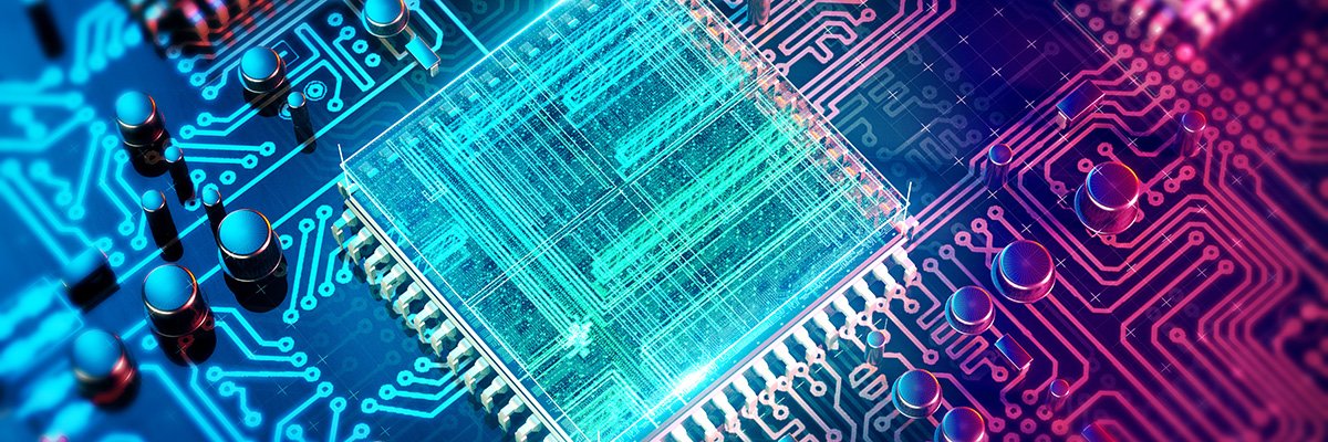
A GPU is an ASIC or Application-Specific Integrated Circuit having a processor (hosting numerous computational cores), a memory soldered onto it (we want to avoid going to the CPU RAM for everything), a cooling system (well, they heat up pretty fast) and a BIOS chip (same role as a CPU — to store settings, run startup diagnostics etc). This card is then plugged into the motherboard slot using the PCI Express interface. The terms GPU and graphics card are often used interchangeably. Some GPUs like the one in Apple M3 do not have a dedicated memory but instead use the system RAM itself which is possible due to its unique design. Google has the TPU (Tensor Processing Unit) which is its own ASIC. We discuss the GPU memory, the processing cores, the LLM workflows happening inside them & common topologies for clustering.
Photo by Thomas Foster on Unsplash
1. GPU Memory module — The VRAM
Instead of having the GPU talk to the regular RAM, it made sense to create another RAM physically closer to the GPU die so that data retrieval is faster. So a graphics card has a memory called VRAM — Video Random Access Memory in addition to the computation engines . VRAM is connected to the computation engine cores via a Bus called the memory interface.
1.1 What is DRAM?
Let us talk first of RAM technology in general. All memory whether it is the CPU RAM or the GPU VRAM are mostly based on DRAM technology which consists of a capacitor and a transistor. The capacitor’s charge represents the data stored. Due to its very nature, this charge gradually leaks. To prevent data loss, a refresh circuit periodically rewrites the data back, restoring its charge. Hence the name — Dynamic RAM due to these preiodic refreshes.
Most computers use Synchronous DDR5 DRAM’s as their CPU RAMs. Synchronous because it utilizes the system clock for better performance. In other words the action (of retrieving & storing data) is operationally coordinated by an external clock signal. Tying the operations to the clock makes it faster. The processor knows the exact timing & number of cycles in which the data will be available from the RAM to the bus & can plan better. We have DDR1 (1st Gen Double Data Rate Synchronous Dynamic RAM released in 2000) to DDR5 which is the choice of CPU RAM as of today.
1.2 What is SGRAM?
Let us now talk about the VRAMs in GPUs. The VRAM is a type of SGRAM — Synchronous Graphics RAM. The current generation of VRAMs being used is GDDR6. Yes, this is 6th generation GDDR, the G standing for “Graphics”. While DDR & GDDR share common origins and early couple of generations were similar, the branches separated after DDR3. So as of 2025, DDR5 rules in CPU RAM and GDDR6 rules for consumer-grade GPU RAMs.
Conceptually DDRs and GDDRs are similar but note that DDRs are used by CPUs which need low latency whereas GDDRs are used by GPUs which are OK to compromise latency for extremely high throughput. Crudely, the former has more frequent smaller calculations & the latter deals with much higher volume of data & some delays are forgiven considering the vast volumes of data being processed. Even more crudely, the former is a bullet train with 6–8 coaches while the latter a 3 Kilometre long goods train.
1.3 GDDR VRAMs explained in detail
GDDR memory are individual chips soldered to the PCB (Printed Circuit Board) very close to the GPU die. The physical proximity improves the speed of data transfer from the VRAM to the GPU processor. There are pins in a GDDR which can be thought of as individual wires that connect it to the processor. Bus width is literally the number of such connections. GDDR6 has 32 pins spread across 2 channels with roughly 16 Gbits.p.s bandwidth per pin. Bandwidth is total amount of data being moved & if you had one single metric at your disposal to take a decision, it would be this. Before we go further, let us try to understand this metric intuitively.
1.4 Calculating GPU Memory Bandwidth intuitively
Memory Bandwidth is the max rate at which data can be transferred between the GPU and the VRAM. We discussed that data transmission is synchronized with the clock. The clock cycle is measured in hertz & represents the number of cycles per second. Let us say we have a clock operating at 1000 MHz. This literally means 1 billion clock ticks per second. How long does a tick last? Literally 1/(1 billion) i.e. 1 nano second. Data is sent to and fro every clock cycle. So every nano-second, a bus-full of data is sent from the VRAM to the processor & vice versa.
How many seats on the bus? Well, we discussed this earlier… This is the memory interface or the bus width… literally the physical count of bits that fit into the bus. A 128-bit bus would ferry 128 bits every nano-second. The D in G’D’DR6 stands for Double. Basically, data is transmitted on both the rising and falling edges of the clock cycle, so 256 bits every nano-second. How many bytes in 1 sec? 256/8 i.e. 32 billion bytes per second or better still 32 GB/s as Giga is the preferred term when measuring data. The capital B denotes bytes whereas the small b denotes bits… a source of confusion.
A more practical formula is: Bandwidth = Clock * Bus Width x Data Rate, where the Data Rate is the number of data transfers per cycle. GDDR6 is Double Data Rate (as just discussed) and Quad pumped, which quadruples the (doubled) speed. So effectively the Data Rate is 8. Sometimes, you may encounter the same information crouched in different semantics. E.g., if frequency of command clock (CK#) is N, then the write command clock (WK#) is 2N. GDDR6 rates then are QDR (quad data rate) in reference to WK# and ODR (Octal Data Rate) in reference to the CK#.
Some OEMs multiply the clock speed & data rate & call it a clock rate or something. In that case, the bandwidth is simply that number multiplied by the bus width. In general, this raw formula can be used: num_of_transfers per second * num_of_bits per transfer / 8. “Boost clock” mechanism allows the GPU and GDDR memory to operate at even higher speeds than the default clock when conditions allow it. Boost clock metric refers to the max such operating clock speed. A 1750 MHz clock means:
1.75GHz is the frequency of command clock(CK#).
The frequency of the write clock (WK#) is 3.5GHz due to the G”D”DR
The Quad pumping takes it to 3.5*4=14 G bits moved in 1 second from each pin on the bus.
We could have bus widths of up to 384 bits! So we get a bandwidth of 14*384 Giga bits per second.
Divide by 8 to get 672 GB/s. GDDR6 bandwidth can go upto 1 TB/s. Wow!
1.5 What is HBM VRAM in a GPU?
When reading or writing data, contention is created when the VRAM has occupied memory channels & is busy receiving or delivering other data. This contention creates latency & this affects bandwidth. Increasing the number of memory channels is a great option. A type of memory called HBM (High-Bandwidth Memory) has lower access latency than GDDR6, since it has 8-memory channels versus 2 channels in GDDR6. HBM also has a wider bus.
HBM has 1024 pins spread across 8 channels of 128 pins with roughly 2 Gbits.p.s bandwidth per pin. Compare this with (an equivalent) GDDR which has 32 pins spread across 2 channels with roughly 16 Gbits. p.s bandwidth per pin. Notice how HBM keeps the Gbit/sec per pin much lower than GDDR. This saves power (which is important as we shall see). In spite of this, it has higher bandwidth than GDDR6 due to the wider bus & higher channels.
As we discussed, a pin is literally a wire connecting the VRAM to the processor. Having 1024 wires connected from the processor to the VRAM is not possible on a standard PCB. Therefore, an “interposer” is used as an
intermediary to connect the VRAM & the processor. Just like a regular IC, wires (connections) are etched in this silicon “interposer” in the desired quantity. After this, the HBM device(s) & the processor are mounted atop this “interposer”. The slightly twisted workaround is called a 2.5D architecture.Another difference is that while GDDR chips are soldered to the PCB surrounding the GPU die, an HBM structure is a vertical stack of DRAMs like a high rise building. The stacked memory dies are linked using microscopic wires with TSV (Through-Silicon Vias) which are vertical electrical connections giving super fast connectivity between the DRAMs. There are huge challenges to stacking items vertically especially around designing heat sinks & managing thermal safety but somehow HBM manufacturers have made this happen.
HBM has become a gold standard today for AI data centers. It was introduced to the Market by SK Hynix in 2013. Today, we have the 3rd generation HBM3 and their main client is Nvidia. Due to investments made way back, SK Hynix is leading the pack along with Samsung and a relatively recent entrant named Micron. We hear a lot about chips and TSMC but HBM is a key technology to watch out for in the coming years. We typically have more than one HBM devices inside the GPU die.
GDDR6 co-exists with HBM3. The markets are complementary. The former addresses PCs & other consumer GPUs whereas the latter addresses data center GPUs. Ultra large scale AI deployments like ChatGPT likely leverage the use of a cluster of NVIDIA GPUs working in tandem. Connecting such GPU’s involves the use of NVIDIA NVLink technology which requires fast GPU memory bandwidth speeds and it’s the reason why HBM is prevalent in such systems. If not for the wide bus width and fast data transfer rates offered by HBM, these kind of clusters would be very difficult to design.
Besides the VRAM, GPUs also include high-speed memory caches that are even closer to the GPU’s processing cores. There is a physical limit to the sizes of these caches. An L1 cache is usually in KB and an L2 cache is usually a few MB. Different hardware & software strategies exist to keep the most useful, and most reused data present in caches.
2. Cooling Mechanisms in a GPU
Higher clock speeds generally result in increased heat generation necessitating the need for cooling solutions to maintain optimal operating temperatures. Usual cooling methods are:
Passive Cooling: These do not have any powered moving components. They take advantage of optimized airflow to take heat away.
Fans are used to dissipate heat by blowing cool air across the heat sinks, which are metal components designed to absorb & disperse heat
In water cooling, water is circulated through the GPU surface using pipes & a radiator. The hot liquid running through the pipes is in turn cooled down by the radiator fan.
Hybrid cooling — which uses a combination of the above
3. GPU Computation cores — Processors
Let us now talk about the processors on the GPU. Unlike CPUs which contain only a few cores, the GPU literally has 1000’s of cores & specializes in running tasks in parallel across these cores using SIMD (Single Instruction, Multiple Data) units. Let us stick to NVIDIA terminology. There are multiple processing units called Streaming Multiprocessor (SM) on a NVIDIA GPU. For e.g. an H100 has upto 144 SMs. What is inside an SM? Well there are mainly 2 type of execution units — CUDA cores & Tensor cores. There is also a small memory SRAM which is Shared between all threads running in that SM. More specifically, every SM has a few KB memory that is partitioned between L1 cache & Shared Memory usage.
3.1 CUDA core versus Tensor core in a GPU — The difference
Tensor cores are a pretty recent innovation (from V100 onwards) and are specifically designed for faster matrix multiplication. Let us discuss CUDA cores first. These are the computation engines for regular math operations. Each CUDA core can execute one operation per clock cycle. But their strength lies in parallel processing. Many CUDA cores working together can accelerate computation by executing processes in parallel.
Tensor Cores are specialized hardware units designed to accelerate “mixed precision” training. The earliest version allowed 4×4 FP16 matrices to be multiplied & added to an FP32 output matrix. By using lower-precision FP16 inputs in the computations, the calculations are vastly accelarated & by retaining FP32 outputs for the rest of the procedure, accuracy is not compromised too much. Modern tensor cores use even lower precision formats in DL computations. See this for more details. There may also specialized units like the transformer engine designed to accelerate models built with the Transformer blocks. A single GPU can be partitioned into multiple fully contained and isolated instances, with their own memory, cache & cores via MIG or Multi Instance GPU technology.
3.2 GPU operations — A FLOP show
Let us now talk about actual operations. A FLOP (Floating Point Operation) is a single floating-point calculation like an addition. Performance of a GPU is usually measured in TeraFLOP/s. Tera is a trillion, FLOP stands for floating-point operations and the ‘s’ stands for per second.
Most matrix ops involve a multiply and an add. It makes sense to fuse these ops together to get an Fused Multiply-Add (FMA) op. If we know the FMA speed, we can simply double it to get the FLOP counts per clock. To get the peak FLOP/s rate, we multiply this by the clock rate & the number of SMs. Note that we have FP16, FP32, FP64 & Int8 cores with varying speeds. For e.g.:
Say there are 4 tensor cores in each SM & 114 SMs in an H100
Say each tensor core delivers 512 FP16 FMA ops per clock. Careful here: Read the specs clearly to check whether the FMA ops per clock metric is per SM or per individual core. For e.g., this link of A100 is per coreper SM
Let the Clock speed = 1620 MHz
So TFLOP/s = 1620 * (2*512) * 4 * 114= 756 TFLOP/s of performance! 756 Trillion operations per second. Wow! What would Babbage say to that?
4. Putting everything together — LLM Operations in a GPU
Given this immense compute-power, we can now make a reasonable guess that LLM inference is memory-I0 bound, not compute bound. In other words, it takes more time to load data to the GPU’s compute cores than it does for those cores to perform LLM computations on that data. The processing itself is super-fast & there is enough & more compute power available.
To start with, the training data needs to be downloaded from a remote source to the CPU memory
From there, it needs to be transferred to the GPU via the system bus and PCIe bus. The host(CPU)-to-device(GPU) bandwidth is limited by the CPU frequency, PCIe bus, GPU devices & the number of PCIe lanes available.
Once the data & weights are in the GPU VRAM, they are then ferried across to the SRAM where the processors perform operations on it.
After the operation the data is moved back to the VRAM & from there it is moved back to the CPU RAM. This is a rather simplistic view. Inside the GPU, the tensors are repeatedly moved back and forth between VRAM & SRAM (the memory allocated to an SM). Can you guess why?
We saw that SRAM size is in KB so large matrices are not going to fit in there … which explains why there is a constant movement between VRAM which holds all the tensors and SRAM which holds the data on which compute operations are performed. So there is typically a memory-op where tensors are moved from VRAM to SRAM, then a compute-op SRAM and memory-op to move tensors back from SRAM to VRAM. Computations like a matrix multiplication involving 2 large matrices need several such memory + compute ops before the action is completed.
During the training of GPT-3, the tensor cores on the GPUs used were found to be idle ~50% of the time. So, to extract the best from the infrastructure, data movement needs to be fast enough to ensure the computation cores are kept reasonably occupied. Surely, there is scope for some smart person to come up with shortcuts. Enter Flash attention & other such hacks. But that is a story for another day!
5. Linking GPUs for LLM training — Topologies
While LLM inferencing is manegable with a readymade collection of GPUs such as a DGX server (contains 8 H100s), LLM training needs far more GPUs. Before we discuss how to connect GPUs for larger workloads, it makes sense to see how CPU servers are connected in a datacentre. I am not an expert in this area, so please feel free to point out any incorrect interpretations I may have made from the references I quote.
5.1 Generic concepts on linking processors
Each server has a card attached to it called the Network Interface Card (NIC). RDMA technology enables direct memory access to a remote server via the NIC hardware. RoCE (RDMA over Converged Ethernet) protocol uses the RDMA technology & adapts it to Ethernet networks. So now, a server can talk to a remote server over a network. A network switch is a device connecting multiple servers in a network, enabling them to communicate with each other. This is the basic technology. Now let us come to the topology.
So we assemble all the servers physically in one place and pile them up vertically them in neat racks.A very basic topology is to connect each server in a rack to a switch that usually sits on Top of the Rack, aptly named the ToR switch. The ToR switches of different racks are connected to a Spine switch. This topology is a basic implementation of Clos topology — named after Charles Clos who invented this scheme to originally arrange telephone nodes in a “leaf-n-spine” arrangement. The leaf switches are nothing but the ToR switches in modern data centers.
Source: Fig 1–1 from
https://www.oreilly.com/library/view/bgp-in-the/9781491983416/ch01.html
Fat tree is a variant of Clos. Like before, we have servers arranged into racks connecting to Top-of-the-Rack (ToR) switches. ToR switches are connected to the aggregation switches to provide connectivity across racks, forming a pod. The pods are interconnected with spine switches, allowing any-to-any communication across servers. To be noted is the fact that there are multiple paths connecting servers. So there is lot of redundancy built-in.
In a typical App deployment running hundreds of microservices on dozens of servers, it is useful to have such fully connected, high bandwidth networks. You never know who is going to talk to whom so it never hurts to overprovision on bandwidth and connectivity. However, network loads during AI training do not follow these patterns. They are more predictable & this allows us to build optimized, cheaper & less power-hungry networks.
5.2 Linking GPUs via proprietary technology like NVLink
We can strap together H100’s by leveraging the proprietary NVLink & NVSwitch technologies. NVLink provides the high-speed connection between individual GPUs, while NVSwitch is a chip that enables multiple GPUs to communicate through NVLink, forming a high-bandwidth network. See this nice article for details.
NVIDIA’s P100 GPU introduced the NVLink1. At that time there was no NVSwitch chip, and the GPUs were connected in a ring-like configuration, which resulted in a lack of direct point-to-point communication between GPUs. The NVSwitch1 chip was introduced with the V100, followed by the NVSwitch2 chip with the A100 GPU. We are in the third-generation NVSwitch3 which can support a cluster of up to 256 H100 GPUs. Each H100 GPU in such a cluster is connected to the internal NVSwitch3 chip through 18 NVLink4.0 connections. This is how trillion parameter LLMs are inferenced.
5.3 Linking GPUs via RoCE in a rail-optimized topology
But as they say, ye dil mange more… Meta reportedly trains its newer models on a cluster that’s over 100K H100’s. Phew! How to they manage to link it all up? The standard NVLink tricks can only scale to a limited number of GPUs. Beyond that, we have to use the network topologies discussed earlier & fall back on technologies like RoCE, which allows data to be directly transferred from one GPU’s memory to another without involving the CPU.
So you have 8 GPUs in one DGX server. You have several such DGX servers in the data centre. Each GPU is assigned a NIC (yes!) & connected via RDMA to all other GPUs thru’ a variant of Clos network called “rail-optimized network”. The idea here is to set up dedicated connections between groups of GPUs with rail switches. If a GPU wants to communicate with a GPU which is in a different group, then it has to go thru’ the spine switch (which takes a lil more time). To implement this, each GPU in a DGX server is indexed serially. A rail is the set of GPUs with the same index on different servers & these are interconnected with a rail switch via RDMA. These rail switches are subsequently connected to spine switches forming any-to-any GPU network.
Source: Fig 1 from
https://arxiv.org/pdf/2307.12169
This topology streamlines traffic flow. It is like having dedicated lanes for high speed vehicles instead of generally mixing all traffic together. Rail paths are direct connections between a bunch of GPUs with same index. Spine switches serve as the connecting points for differently-indexed GPUs. For e.g., communication between GPU1 of server 1 and GPU1 of server 2 happens via their dedicated rail switch 1. If GPU1 of server 1 needs to reach GPU5 of another server, it has to go thru’ a spine switch.
The workloads are designed so as to minimize data transfers across rails (since it has to go thru’ the extra spine switch). The good news is that this can be neatly done for AI training ensuring that most of the traffic stays within the rails, and does not cut across. In fact, there is a recent paper which suggests that you can consider removing costly spine switches altogether as inter-rail communication is minimal. Can you guess how?
5.4 Linking GPUs via RoCE in a rail-only topology
Well, we have the superfast connectivity using NVLink to communicate between a limited set of GPUs (upto 256). So you create these High Bandwith (HB) domains which use NVLink for communication. You have several such HB domains. We then have the same indexing system and rail connections to interconnect the HB domains. But there are no spine switches! Can you guess how GPU1 of HB domain 1 can talk to GPU5 of another HB domain? Yes! Transfer data via superfast NVLink to GPU5 of HB domain 1 first. Then use the dedicated rail of GPU5 to talk to the GPU5 in another HB domain! This is a rail-only topology as oppsed to rail-optimized topology!
Given these topologies, we can now plan the training pipeline to have pipeline parallelism, tensor parallelism &/or data parallelism but that is a story for another day. See this, this & this for more details. 100K H100’s consume a LOT of power. Tech companies are exploring nuclear power options to generate clean energy needed for long term sustenance. Else, a 100K GPU cluster may have to be broken down to smaller clusters and connected using optical transceivers across the buildings in a campus.
This (unplanned) article is a prelude to — Optimizing LLM inference: Key Faultlines & workarounds. To deeply understand how we can optimize LLM operations, we need to understand more about the silicon on which they are executed. Though there are lots of manuals/guides on individual aspects like memory, processors, networking etc, I couldn’t find a concise and reader-friendly thread linking together these various aspects & hence took a shot. This is the 9th of a 15-series article titled My LLM diaries.
LLM Quantization — From concepts to implementation
LoRA & its newer variants explained like never before
In-Context learning: The greatest magic show in the kingdom of LLMs
RAG in plain English — Summary of 100+ papers
HNSW — Story of the world’s most popular Vector search algorithm
VectorDB origins, Vamana & on-disk Vector search algorithms
Taming LLMs — A study of few popular techniques
Understanding LLM Agents: Concepts, Patterns & Frameworks
Anatomy of a GPU — A peek into the hardware fuelling LLM operations
Optimizing LLM Inference — Key Faultlines & workarounds
LLM Serving — Architecture considerations
LLM evaluation & other odds and ends
Look Ma, LLMs without Prompt Engineering
LLMs on the laptop — A peek into the Silicon
Taking a step back — On model sentience, conscientiousness & other philosophical aspects
Join thousands of data leaders on the AI newsletter. Join over 80,000 subscribers and keep up to date with the latest developments in AI. From research to projects and ideas. If you are building an AI startup, an AI-related product, or a service, we invite you to consider becoming a sponsor.
Published via Towards AI
المصدر:
https://towardsai.net/p/machine-learning/gpu-architecture-working-intuitively-explainedGPU Architecture & Working intuitively explained
Author(s): Allohvk
Originally published on Towards AI.
GPU Origins
The image displayed on a computer screen is made up of millions of tiny pixels. In early days, “graphics controllers” were given instructions by the CPU on how to calculate the individual pixel values so that the appropriate image could be displayed. These were ok for conventional displays but for a really good gaming experience, images need to be built dozens of times per second. The CPU was not really designed to handle these kind of loads.
The whole process of creating the image could be parallelized big-time simply by (a) dividing the image into smaller blocks (b) carrying out computations for each block in parallel & (c) grouping them back again. The results of one block don’t influence the results of the other blocks. CPU’s multi-threading capabilities was not really conceived for such massive parallelization. Enter the GPU! Sony first used the term GPU in 1994, in its PlayStation consoles. The technology was perfected by NVIDIA which soon became a leader.
GPUs have numerous computation cores (much more than a CPU) and gaming programmers could write Shaders — programs to run graphics computations on the GPU in a massively parallelized way to create the screen images in super-fast time. The GPU is inspired by the CPU but was specifically designed to enable massive multi-threaded operations on its numerous computation cores seamlessly. Creating threads, switching between threads etc is much faster on a GPU. Some smart developers also realized that these parallel processing capabilities could be used for other computationally intensive tasks as well!
2005: Steinkrau implements a simple 2-layer Neural Net on a GPU
2006: Kumar et. al. trains a CNN model for document processing
2007: NVIDIA released Compute Unified Device Architecture (CUDA) — a custom language extending C to exploit data parallelism on GPUs. Now developers had much more granular control over the image rendering.
2008 a landmark paper by Raina et al was released. This paper pretty much showed everyone how to train deep layers on a GPU
2014: NVIDIA released CuDNN — a dedicated CUDA library for Deep Learning. Very soon PyTorch, TensorFlow etc incorporated CuDNN, setting the stage for modern GPU usage for AI!
A GPU is an ASIC or Application-Specific Integrated Circuit having a processor (hosting numerous computational cores), a memory soldered onto it (we want to avoid going to the CPU RAM for everything), a cooling system (well, they heat up pretty fast) and a BIOS chip (same role as a CPU — to store settings, run startup diagnostics etc). This card is then plugged into the motherboard slot using the PCI Express interface. The terms GPU and graphics card are often used interchangeably. Some GPUs like the one in Apple M3 do not have a dedicated memory but instead use the system RAM itself which is possible due to its unique design. Google has the TPU (Tensor Processing Unit) which is its own ASIC. We discuss the GPU memory, the processing cores, the LLM workflows happening inside them & common topologies for clustering.
Photo by Thomas Foster on Unsplash
1. GPU Memory module — The VRAM
Instead of having the GPU talk to the regular RAM, it made sense to create another RAM physically closer to the GPU die so that data retrieval is faster. So a graphics card has a memory called VRAM — Video Random Access Memory in addition to the computation engines . VRAM is connected to the computation engine cores via a Bus called the memory interface.
1.1 What is DRAM?
Let us talk first of RAM technology in general. All memory whether it is the CPU RAM or the GPU VRAM are mostly based on DRAM technology which consists of a capacitor and a transistor. The capacitor’s charge represents the data stored. Due to its very nature, this charge gradually leaks. To prevent data loss, a refresh circuit periodically rewrites the data back, restoring its charge. Hence the name — Dynamic RAM due to these preiodic refreshes.
Most computers use Synchronous DDR5 DRAM’s as their CPU RAMs. Synchronous because it utilizes the system clock for better performance. In other words the action (of retrieving & storing data) is operationally coordinated by an external clock signal. Tying the operations to the clock makes it faster. The processor knows the exact timing & number of cycles in which the data will be available from the RAM to the bus & can plan better. We have DDR1 (1st Gen Double Data Rate Synchronous Dynamic RAM released in 2000) to DDR5 which is the choice of CPU RAM as of today.
1.2 What is SGRAM?
Let us now talk about the VRAMs in GPUs. The VRAM is a type of SGRAM — Synchronous Graphics RAM. The current generation of VRAMs being used is GDDR6. Yes, this is 6th generation GDDR, the G standing for “Graphics”. While DDR & GDDR share common origins and early couple of generations were similar, the branches separated after DDR3. So as of 2025, DDR5 rules in CPU RAM and GDDR6 rules for consumer-grade GPU RAMs.
Conceptually DDRs and GDDRs are similar but note that DDRs are used by CPUs which need low latency whereas GDDRs are used by GPUs which are OK to compromise latency for extremely high throughput. Crudely, the former has more frequent smaller calculations & the latter deals with much higher volume of data & some delays are forgiven considering the vast volumes of data being processed. Even more crudely, the former is a bullet train with 6–8 coaches while the latter a 3 Kilometre long goods train.
1.3 GDDR VRAMs explained in detail
GDDR memory are individual chips soldered to the PCB (Printed Circuit Board) very close to the GPU die. The physical proximity improves the speed of data transfer from the VRAM to the GPU processor. There are pins in a GDDR which can be thought of as individual wires that connect it to the processor. Bus width is literally the number of such connections. GDDR6 has 32 pins spread across 2 channels with roughly 16 Gbits.p.s bandwidth per pin. Bandwidth is total amount of data being moved & if you had one single metric at your disposal to take a decision, it would be this. Before we go further, let us try to understand this metric intuitively.
1.4 Calculating GPU Memory Bandwidth intuitively
Memory Bandwidth is the max rate at which data can be transferred between the GPU and the VRAM. We discussed that data transmission is synchronized with the clock. The clock cycle is measured in hertz & represents the number of cycles per second. Let us say we have a clock operating at 1000 MHz. This literally means 1 billion clock ticks per second. How long does a tick last? Literally 1/(1 billion) i.e. 1 nano second. Data is sent to and fro every clock cycle. So every nano-second, a bus-full of data is sent from the VRAM to the processor & vice versa.
How many seats on the bus? Well, we discussed this earlier… This is the memory interface or the bus width… literally the physical count of bits that fit into the bus. A 128-bit bus would ferry 128 bits every nano-second. The D in G’D’DR6 stands for Double. Basically, data is transmitted on both the rising and falling edges of the clock cycle, so 256 bits every nano-second. How many bytes in 1 sec? 256/8 i.e. 32 billion bytes per second or better still 32 GB/s as Giga is the preferred term when measuring data. The capital B denotes bytes whereas the small b denotes bits… a source of confusion.
A more practical formula is: Bandwidth = Clock * Bus Width x Data Rate, where the Data Rate is the number of data transfers per cycle. GDDR6 is Double Data Rate (as just discussed) and Quad pumped, which quadruples the (doubled) speed. So effectively the Data Rate is 8. Sometimes, you may encounter the same information crouched in different semantics. E.g., if frequency of command clock (CK#) is N, then the write command clock (WK#) is 2N. GDDR6 rates then are QDR (quad data rate) in reference to WK# and ODR (Octal Data Rate) in reference to the CK#.
Some OEMs multiply the clock speed & data rate & call it a clock rate or something. In that case, the bandwidth is simply that number multiplied by the bus width. In general, this raw formula can be used: num_of_transfers per second * num_of_bits per transfer / 8. “Boost clock” mechanism allows the GPU and GDDR memory to operate at even higher speeds than the default clock when conditions allow it. Boost clock metric refers to the max such operating clock speed. A 1750 MHz clock means:
1.75GHz is the frequency of command clock(CK#).
The frequency of the write clock (WK#) is 3.5GHz due to the G”D”DR
The Quad pumping takes it to 3.5*4=14 G bits moved in 1 second from each pin on the bus.
We could have bus widths of up to 384 bits! So we get a bandwidth of 14*384 Giga bits per second.
Divide by 8 to get 672 GB/s. GDDR6 bandwidth can go upto 1 TB/s. Wow!
1.5 What is HBM VRAM in a GPU?
When reading or writing data, contention is created when the VRAM has occupied memory channels & is busy receiving or delivering other data. This contention creates latency & this affects bandwidth. Increasing the number of memory channels is a great option. A type of memory called HBM (High-Bandwidth Memory) has lower access latency than GDDR6, since it has 8-memory channels versus 2 channels in GDDR6. HBM also has a wider bus.
HBM has 1024 pins spread across 8 channels of 128 pins with roughly 2 Gbits.p.s bandwidth per pin. Compare this with (an equivalent) GDDR which has 32 pins spread across 2 channels with roughly 16 Gbits. p.s bandwidth per pin. Notice how HBM keeps the Gbit/sec per pin much lower than GDDR. This saves power (which is important as we shall see). In spite of this, it has higher bandwidth than GDDR6 due to the wider bus & higher channels.
As we discussed, a pin is literally a wire connecting the VRAM to the processor. Having 1024 wires connected from the processor to the VRAM is not possible on a standard PCB. Therefore, an “interposer” is used as an
intermediary to connect the VRAM & the processor. Just like a regular IC, wires (connections) are etched in this silicon “interposer” in the desired quantity. After this, the HBM device(s) & the processor are mounted atop this “interposer”. The slightly twisted workaround is called a 2.5D architecture.Another difference is that while GDDR chips are soldered to the PCB surrounding the GPU die, an HBM structure is a vertical stack of DRAMs like a high rise building. The stacked memory dies are linked using microscopic wires with TSV (Through-Silicon Vias) which are vertical electrical connections giving super fast connectivity between the DRAMs. There are huge challenges to stacking items vertically especially around designing heat sinks & managing thermal safety but somehow HBM manufacturers have made this happen.
HBM has become a gold standard today for AI data centers. It was introduced to the Market by SK Hynix in 2013. Today, we have the 3rd generation HBM3 and their main client is Nvidia. Due to investments made way back, SK Hynix is leading the pack along with Samsung and a relatively recent entrant named Micron. We hear a lot about chips and TSMC but HBM is a key technology to watch out for in the coming years. We typically have more than one HBM devices inside the GPU die.
GDDR6 co-exists with HBM3. The markets are complementary. The former addresses PCs & other consumer GPUs whereas the latter addresses data center GPUs. Ultra large scale AI deployments like ChatGPT likely leverage the use of a cluster of NVIDIA GPUs working in tandem. Connecting such GPU’s involves the use of NVIDIA NVLink technology which requires fast GPU memory bandwidth speeds and it’s the reason why HBM is prevalent in such systems. If not for the wide bus width and fast data transfer rates offered by HBM, these kind of clusters would be very difficult to design.
Besides the VRAM, GPUs also include high-speed memory caches that are even closer to the GPU’s processing cores. There is a physical limit to the sizes of these caches. An L1 cache is usually in KB and an L2 cache is usually a few MB. Different hardware & software strategies exist to keep the most useful, and most reused data present in caches.
2. Cooling Mechanisms in a GPU
Higher clock speeds generally result in increased heat generation necessitating the need for cooling solutions to maintain optimal operating temperatures. Usual cooling methods are:
Passive Cooling: These do not have any powered moving components. They take advantage of optimized airflow to take heat away.
Fans are used to dissipate heat by blowing cool air across the heat sinks, which are metal components designed to absorb & disperse heat
In water cooling, water is circulated through the GPU surface using pipes & a radiator. The hot liquid running through the pipes is in turn cooled down by the radiator fan.
Hybrid cooling — which uses a combination of the above
3. GPU Computation cores — Processors
Let us now talk about the processors on the GPU. Unlike CPUs which contain only a few cores, the GPU literally has 1000’s of cores & specializes in running tasks in parallel across these cores using SIMD (Single Instruction, Multiple Data) units. Let us stick to NVIDIA terminology. There are multiple processing units called Streaming Multiprocessor (SM) on a NVIDIA GPU. For e.g. an H100 has upto 144 SMs. What is inside an SM? Well there are mainly 2 type of execution units — CUDA cores & Tensor cores. There is also a small memory SRAM which is Shared between all threads running in that SM. More specifically, every SM has a few KB memory that is partitioned between L1 cache & Shared Memory usage.
3.1 CUDA core versus Tensor core in a GPU — The difference
Tensor cores are a pretty recent innovation (from V100 onwards) and are specifically designed for faster matrix multiplication. Let us discuss CUDA cores first. These are the computation engines for regular math operations. Each CUDA core can execute one operation per clock cycle. But their strength lies in parallel processing. Many CUDA cores working together can accelerate computation by executing processes in parallel.
Tensor Cores are specialized hardware units designed to accelerate “mixed precision” training. The earliest version allowed 4×4 FP16 matrices to be multiplied & added to an FP32 output matrix. By using lower-precision FP16 inputs in the computations, the calculations are vastly accelarated & by retaining FP32 outputs for the rest of the procedure, accuracy is not compromised too much. Modern tensor cores use even lower precision formats in DL computations. See this for more details. There may also specialized units like the transformer engine designed to accelerate models built with the Transformer blocks. A single GPU can be partitioned into multiple fully contained and isolated instances, with their own memory, cache & cores via MIG or Multi Instance GPU technology.
3.2 GPU operations — A FLOP show
Let us now talk about actual operations. A FLOP (Floating Point Operation) is a single floating-point calculation like an addition. Performance of a GPU is usually measured in TeraFLOP/s. Tera is a trillion, FLOP stands for floating-point operations and the ‘s’ stands for per second.
Most matrix ops involve a multiply and an add. It makes sense to fuse these ops together to get an Fused Multiply-Add (FMA) op. If we know the FMA speed, we can simply double it to get the FLOP counts per clock. To get the peak FLOP/s rate, we multiply this by the clock rate & the number of SMs. Note that we have FP16, FP32, FP64 & Int8 cores with varying speeds. For e.g.:
Say there are 4 tensor cores in each SM & 114 SMs in an H100
Say each tensor core delivers 512 FP16 FMA ops per clock. Careful here: Read the specs clearly to check whether the FMA ops per clock metric is per SM or per individual core. For e.g., this link of A100 is per coreper SM
Let the Clock speed = 1620 MHz
So TFLOP/s = 1620 * (2*512) * 4 * 114= 756 TFLOP/s of performance! 756 Trillion operations per second. Wow! What would Babbage say to that?
4. Putting everything together — LLM Operations in a GPU
Given this immense compute-power, we can now make a reasonable guess that LLM inference is memory-I0 bound, not compute bound. In other words, it takes more time to load data to the GPU’s compute cores than it does for those cores to perform LLM computations on that data. The processing itself is super-fast & there is enough & more compute power available.
To start with, the training data needs to be downloaded from a remote source to the CPU memory
From there, it needs to be transferred to the GPU via the system bus and PCIe bus. The host(CPU)-to-device(GPU) bandwidth is limited by the CPU frequency, PCIe bus, GPU devices & the number of PCIe lanes available.
Once the data & weights are in the GPU VRAM, they are then ferried across to the SRAM where the processors perform operations on it.
After the operation the data is moved back to the VRAM & from there it is moved back to the CPU RAM. This is a rather simplistic view. Inside the GPU, the tensors are repeatedly moved back and forth between VRAM & SRAM (the memory allocated to an SM). Can you guess why?
We saw that SRAM size is in KB so large matrices are not going to fit in there … which explains why there is a constant movement between VRAM which holds all the tensors and SRAM which holds the data on which compute operations are performed. So there is typically a memory-op where tensors are moved from VRAM to SRAM, then a compute-op SRAM and memory-op to move tensors back from SRAM to VRAM. Computations like a matrix multiplication involving 2 large matrices need several such memory + compute ops before the action is completed.
During the training of GPT-3, the tensor cores on the GPUs used were found to be idle ~50% of the time. So, to extract the best from the infrastructure, data movement needs to be fast enough to ensure the computation cores are kept reasonably occupied. Surely, there is scope for some smart person to come up with shortcuts. Enter Flash attention & other such hacks. But that is a story for another day!
5. Linking GPUs for LLM training — Topologies
While LLM inferencing is manegable with a readymade collection of GPUs such as a DGX server (contains 8 H100s), LLM training needs far more GPUs. Before we discuss how to connect GPUs for larger workloads, it makes sense to see how CPU servers are connected in a datacentre. I am not an expert in this area, so please feel free to point out any incorrect interpretations I may have made from the references I quote.
5.1 Generic concepts on linking processors
Each server has a card attached to it called the Network Interface Card (NIC). RDMA technology enables direct memory access to a remote server via the NIC hardware. RoCE (RDMA over Converged Ethernet) protocol uses the RDMA technology & adapts it to Ethernet networks. So now, a server can talk to a remote server over a network. A network switch is a device connecting multiple servers in a network, enabling them to communicate with each other. This is the basic technology. Now let us come to the topology.
So we assemble all the servers physically in one place and pile them up vertically them in neat racks.A very basic topology is to connect each server in a rack to a switch that usually sits on Top of the Rack, aptly named the ToR switch. The ToR switches of different racks are connected to a Spine switch. This topology is a basic implementation of Clos topology — named after Charles Clos who invented this scheme to originally arrange telephone nodes in a “leaf-n-spine” arrangement. The leaf switches are nothing but the ToR switches in modern data centers.
Source: Fig 1–1 from https://www.oreilly.com/library/view/bgp-in-the/9781491983416/ch01.html
Fat tree is a variant of Clos. Like before, we have servers arranged into racks connecting to Top-of-the-Rack (ToR) switches. ToR switches are connected to the aggregation switches to provide connectivity across racks, forming a pod. The pods are interconnected with spine switches, allowing any-to-any communication across servers. To be noted is the fact that there are multiple paths connecting servers. So there is lot of redundancy built-in.
In a typical App deployment running hundreds of microservices on dozens of servers, it is useful to have such fully connected, high bandwidth networks. You never know who is going to talk to whom so it never hurts to overprovision on bandwidth and connectivity. However, network loads during AI training do not follow these patterns. They are more predictable & this allows us to build optimized, cheaper & less power-hungry networks.
5.2 Linking GPUs via proprietary technology like NVLink
We can strap together H100’s by leveraging the proprietary NVLink & NVSwitch technologies. NVLink provides the high-speed connection between individual GPUs, while NVSwitch is a chip that enables multiple GPUs to communicate through NVLink, forming a high-bandwidth network. See this nice article for details.
NVIDIA’s P100 GPU introduced the NVLink1. At that time there was no NVSwitch chip, and the GPUs were connected in a ring-like configuration, which resulted in a lack of direct point-to-point communication between GPUs. The NVSwitch1 chip was introduced with the V100, followed by the NVSwitch2 chip with the A100 GPU. We are in the third-generation NVSwitch3 which can support a cluster of up to 256 H100 GPUs. Each H100 GPU in such a cluster is connected to the internal NVSwitch3 chip through 18 NVLink4.0 connections. This is how trillion parameter LLMs are inferenced.
5.3 Linking GPUs via RoCE in a rail-optimized topology
But as they say, ye dil mange more… Meta reportedly trains its newer models on a cluster that’s over 100K H100’s. Phew! How to they manage to link it all up? The standard NVLink tricks can only scale to a limited number of GPUs. Beyond that, we have to use the network topologies discussed earlier & fall back on technologies like RoCE, which allows data to be directly transferred from one GPU’s memory to another without involving the CPU.
So you have 8 GPUs in one DGX server. You have several such DGX servers in the data centre. Each GPU is assigned a NIC (yes!) & connected via RDMA to all other GPUs thru’ a variant of Clos network called “rail-optimized network”. The idea here is to set up dedicated connections between groups of GPUs with rail switches. If a GPU wants to communicate with a GPU which is in a different group, then it has to go thru’ the spine switch (which takes a lil more time). To implement this, each GPU in a DGX server is indexed serially. A rail is the set of GPUs with the same index on different servers & these are interconnected with a rail switch via RDMA. These rail switches are subsequently connected to spine switches forming any-to-any GPU network.
Source: Fig 1 from https://arxiv.org/pdf/2307.12169
This topology streamlines traffic flow. It is like having dedicated lanes for high speed vehicles instead of generally mixing all traffic together. Rail paths are direct connections between a bunch of GPUs with same index. Spine switches serve as the connecting points for differently-indexed GPUs. For e.g., communication between GPU1 of server 1 and GPU1 of server 2 happens via their dedicated rail switch 1. If GPU1 of server 1 needs to reach GPU5 of another server, it has to go thru’ a spine switch.
The workloads are designed so as to minimize data transfers across rails (since it has to go thru’ the extra spine switch). The good news is that this can be neatly done for AI training ensuring that most of the traffic stays within the rails, and does not cut across. In fact, there is a recent paper which suggests that you can consider removing costly spine switches altogether as inter-rail communication is minimal. Can you guess how?
5.4 Linking GPUs via RoCE in a rail-only topology
Well, we have the superfast connectivity using NVLink to communicate between a limited set of GPUs (upto 256). So you create these High Bandwith (HB) domains which use NVLink for communication. You have several such HB domains. We then have the same indexing system and rail connections to interconnect the HB domains. But there are no spine switches! Can you guess how GPU1 of HB domain 1 can talk to GPU5 of another HB domain? Yes! Transfer data via superfast NVLink to GPU5 of HB domain 1 first. Then use the dedicated rail of GPU5 to talk to the GPU5 in another HB domain! This is a rail-only topology as oppsed to rail-optimized topology!
Given these topologies, we can now plan the training pipeline to have pipeline parallelism, tensor parallelism &/or data parallelism but that is a story for another day. See this, this & this for more details. 100K H100’s consume a LOT of power. Tech companies are exploring nuclear power options to generate clean energy needed for long term sustenance. Else, a 100K GPU cluster may have to be broken down to smaller clusters and connected using optical transceivers across the buildings in a campus.
This (unplanned) article is a prelude to — Optimizing LLM inference: Key Faultlines & workarounds. To deeply understand how we can optimize LLM operations, we need to understand more about the silicon on which they are executed. Though there are lots of manuals/guides on individual aspects like memory, processors, networking etc, I couldn’t find a concise and reader-friendly thread linking together these various aspects & hence took a shot. This is the 9th of a 15-series article titled My LLM diaries.
LLM Quantization — From concepts to implementation
LoRA & its newer variants explained like never before
In-Context learning: The greatest magic show in the kingdom of LLMs
RAG in plain English — Summary of 100+ papers
HNSW — Story of the world’s most popular Vector search algorithm
VectorDB origins, Vamana & on-disk Vector search algorithms
Taming LLMs — A study of few popular techniques
Understanding LLM Agents: Concepts, Patterns & Frameworks
Anatomy of a GPU — A peek into the hardware fuelling LLM operations
Optimizing LLM Inference — Key Faultlines & workarounds
LLM Serving — Architecture considerations
LLM evaluation & other odds and ends
Look Ma, LLMs without Prompt Engineering
LLMs on the laptop — A peek into the Silicon
Taking a step back — On model sentience, conscientiousness & other philosophical aspects
Join thousands of data leaders on the AI newsletter. Join over 80,000 subscribers and keep up to date with the latest developments in AI. From research to projects and ideas. If you are building an AI startup, an AI-related product, or a service, we invite you to consider becoming a sponsor.
Published via Towards AI
المصدر: https://towardsai.net/p/machine-learning/gpu-architecture-working-intuitively-explained