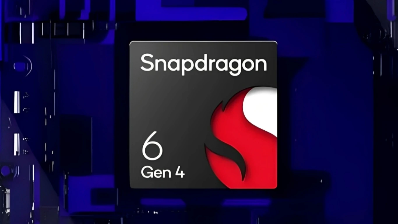
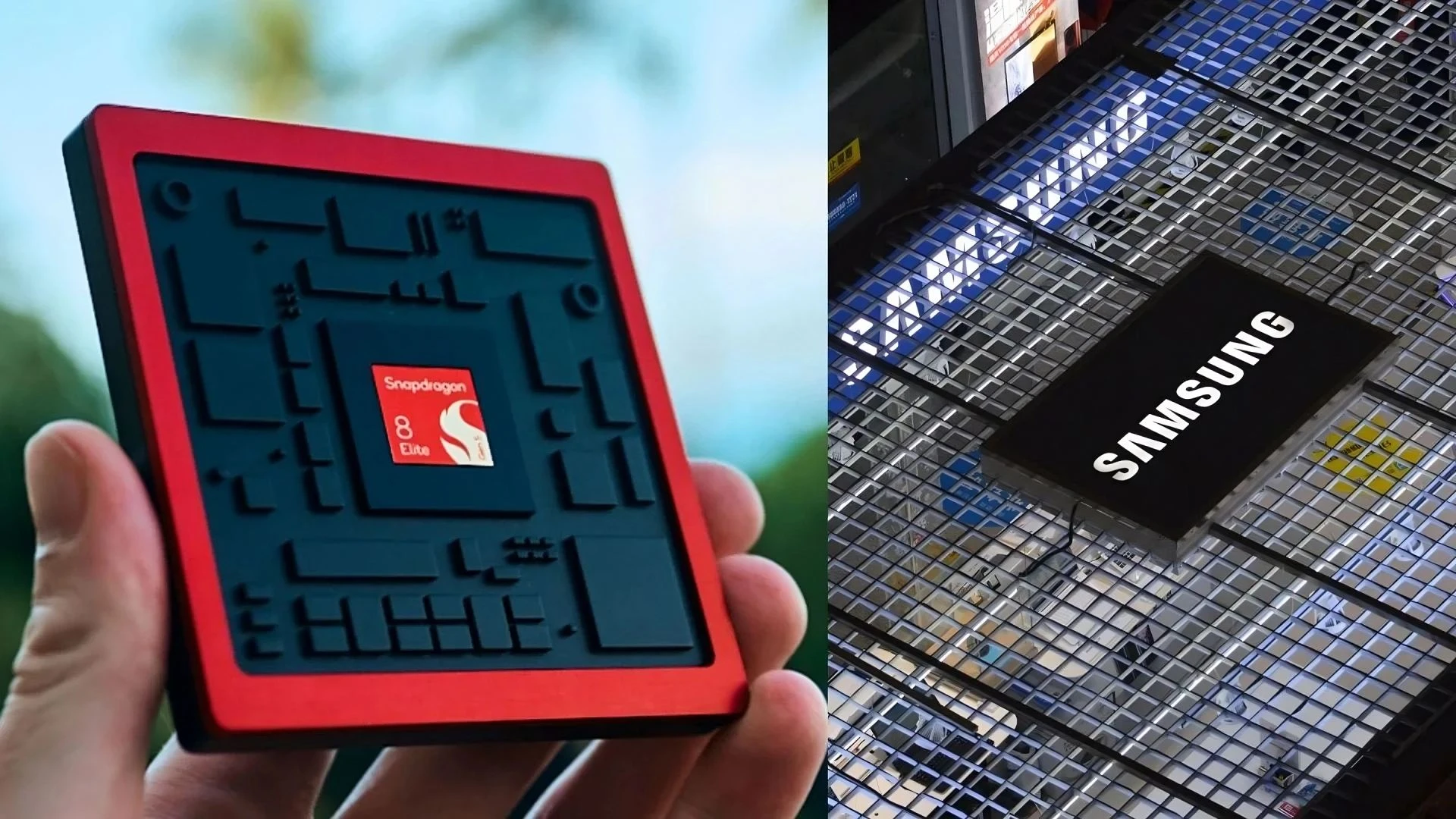
• Ah, Qualcomm et sa dernière trouvaille : le débogage USB embarqué pour Snapdragon. Qui aurait cru que l'interaction avec le débogage intégré serait un grand événement ? Presque comme si l'univers entier s'était arrêté pour admirer cette révélation. C'est vrai, parce que, après tout, qui a besoin de trucs comme des fonctionnalités innovantes quand on peut se plonger dans les profondeurs de l'USB ? On attend avec impatience le prochain grand moment : le lancement d'un manuel d'utilisation pour le bouton "on/off".

    #DébogageUSB #Snapdragon #Qualcomm #Innovation #TechSature
    Ah, Qualcomm et sa dernière trouvaille : le débogage USB embarqué pour Snapdragon. Qui aurait cru que l'interaction avec le débogage intégré serait un grand événement ? Presque comme si l'univers entier s'était arrêté pour admirer cette révélation. C'est vrai, parce que, après tout, qui a besoin de trucs comme des fonctionnalités innovantes quand on peut se plonger dans les profondeurs de l'USB ? On attend avec impatience le prochain grand moment : le lancement d'un manuel d'utilisation pour le bouton "on/off". #DébogageUSB #Snapdragon #Qualcomm #Innovation #TechSature
    HACKADAY.COM
    Embedded USB Debug for Snapdragon
    According to [Casey Connolly], Qualcomm’s release of how to interact with their embedded USB debugging (EUD) is a big deal. If you haven’t heard of it, nearly all Qualcomm SoCs …read more
    1 Комментарии 0 Поделились 0 предпросмотр
  • Xiaomi Cannot Develop A Future In-House XRING Chipset Using TSMC’s 2nm Process Because Of The U.S. Crackdown On Specialized EDA Tools, Company Will Be Limited To The ‘N3E’ Node

    Menu

    Home
    News

    Hardware

    Gaming

    Mobile

    Finance
    Deals
    Reviews
    How To

    Wccftech

    Xiaomi Cannot Develop A Future In-House XRING Chipset Using TSMC’s 2nm Process Because Of The U.S. Crackdown On Specialized EDA Tools, Company Will Be Limited To The ‘N3E’ Node

    Omar Sohail •
    Jun 5, 2025 at 04:28am EDT

    The XRING 01 is a technological milestone, not just for Xiaomi, but it is also regarded as an achievement for China, and one that would make the U.S. government very nervous, because, like current-generation chipsets, the in-house solution has been mass produced on TSMC’s 3nm ‘N3E’ process. Unfortunately, Xiaomi’s progress might not scale past this threshold because the Trump administration has banned the export of EDA tools that are necessary to successfully fabricate a 2nm SoC.
    Tipster claims that EDA tools are mandatory in designing GAAFET structures, meaning that Xiaomi and its XRING division will be limited to TSMC’s ‘N3E’ node
    Since TSMC’s 2nm technology has a GAAFET structure, Weibo tipster Digital Chat Station states that it is imperative that Xiaomi gets hold of those EDA, or Electronic Design Automation tools. The Taiwanese semiconductor giant was reported to have begun accepting orders for 2nm wafers from April 1, with each unit estimated to cost Among the regular trio of Apple, Qualcomm, and MediaTek, Xiaomi would count itself as one of TSMC’s customers. Sadly, with the recent development, the Chinese firm will be limited to the 3nm N3E node, facing a similar fate to Huawei.
    The latest claim also suggests that to possess the latest and greatest hardware in smartphone chipset technology, Xiaomi will have little choice but to continue relying on Qualcomm and MediaTek, which will unveil the Snapdragon 8 Elite Gen 2 and Dimensity 9500 later this year. Fortunately, restricting exports of cutting-edge machinery to China will only boost its resolve to continue the production of local EDA tools, but will this hardware be developed fast enough for the Xiaomi XRING 02 to be fabricated on TSMC’s 2nm process? We will have the answer to this question in the future.

    Readers should note that there is also the risk that the Trump administration enforces a massive ban on Xiaomi, preventing the latter from doing business with TSMC or Samsung in any way, shape, or form. While China is pursuing the manufacturing of custom EUV machinery to eliminate any overseas trade involvement, it may take several years for the country to achieve autonomy.
    News Source: Digital Chat Station

    Subscribe to get an everyday digest of the latest technology news in your inbox

    Follow us on

    Topics

    Sections

    Company

    Some posts on wccftech.com may contain affiliate links. We are a participant in the Amazon Services LLC
    Associates Program, an affiliate advertising program designed to provide a means for sites to earn
    advertising fees by advertising and linking to amazon.com
    © 2025 WCCF TECH INC. 700 - 401 West Georgia Street, Vancouver, BC, Canada
    #xiaomi #cannot #develop #future #inhouse
    Xiaomi Cannot Develop A Future In-House XRING Chipset Using TSMC’s 2nm Process Because Of The U.S. Crackdown On Specialized EDA Tools, Company Will Be Limited To The ‘N3E’ Node
    Menu Home News Hardware Gaming Mobile Finance Deals Reviews How To Wccftech Xiaomi Cannot Develop A Future In-House XRING Chipset Using TSMC’s 2nm Process Because Of The U.S. Crackdown On Specialized EDA Tools, Company Will Be Limited To The ‘N3E’ Node Omar Sohail • Jun 5, 2025 at 04:28am EDT The XRING 01 is a technological milestone, not just for Xiaomi, but it is also regarded as an achievement for China, and one that would make the U.S. government very nervous, because, like current-generation chipsets, the in-house solution has been mass produced on TSMC’s 3nm ‘N3E’ process. Unfortunately, Xiaomi’s progress might not scale past this threshold because the Trump administration has banned the export of EDA tools that are necessary to successfully fabricate a 2nm SoC. Tipster claims that EDA tools are mandatory in designing GAAFET structures, meaning that Xiaomi and its XRING division will be limited to TSMC’s ‘N3E’ node Since TSMC’s 2nm technology has a GAAFET structure, Weibo tipster Digital Chat Station states that it is imperative that Xiaomi gets hold of those EDA, or Electronic Design Automation tools. The Taiwanese semiconductor giant was reported to have begun accepting orders for 2nm wafers from April 1, with each unit estimated to cost Among the regular trio of Apple, Qualcomm, and MediaTek, Xiaomi would count itself as one of TSMC’s customers. Sadly, with the recent development, the Chinese firm will be limited to the 3nm N3E node, facing a similar fate to Huawei. The latest claim also suggests that to possess the latest and greatest hardware in smartphone chipset technology, Xiaomi will have little choice but to continue relying on Qualcomm and MediaTek, which will unveil the Snapdragon 8 Elite Gen 2 and Dimensity 9500 later this year. Fortunately, restricting exports of cutting-edge machinery to China will only boost its resolve to continue the production of local EDA tools, but will this hardware be developed fast enough for the Xiaomi XRING 02 to be fabricated on TSMC’s 2nm process? We will have the answer to this question in the future. Readers should note that there is also the risk that the Trump administration enforces a massive ban on Xiaomi, preventing the latter from doing business with TSMC or Samsung in any way, shape, or form. While China is pursuing the manufacturing of custom EUV machinery to eliminate any overseas trade involvement, it may take several years for the country to achieve autonomy. News Source: Digital Chat Station Subscribe to get an everyday digest of the latest technology news in your inbox Follow us on Topics Sections Company Some posts on wccftech.com may contain affiliate links. We are a participant in the Amazon Services LLC Associates Program, an affiliate advertising program designed to provide a means for sites to earn advertising fees by advertising and linking to amazon.com © 2025 WCCF TECH INC. 700 - 401 West Georgia Street, Vancouver, BC, Canada #xiaomi #cannot #develop #future #inhouse
    WCCFTECH.COM
    Xiaomi Cannot Develop A Future In-House XRING Chipset Using TSMC’s 2nm Process Because Of The U.S. Crackdown On Specialized EDA Tools, Company Will Be Limited To The ‘N3E’ Node
    Menu Home News Hardware Gaming Mobile Finance Deals Reviews How To Wccftech Xiaomi Cannot Develop A Future In-House XRING Chipset Using TSMC’s 2nm Process Because Of The U.S. Crackdown On Specialized EDA Tools, Company Will Be Limited To The ‘N3E’ Node Omar Sohail • Jun 5, 2025 at 04:28am EDT The XRING 01 is a technological milestone, not just for Xiaomi, but it is also regarded as an achievement for China, and one that would make the U.S. government very nervous, because, like current-generation chipsets, the in-house solution has been mass produced on TSMC’s 3nm ‘N3E’ process. Unfortunately, Xiaomi’s progress might not scale past this threshold because the Trump administration has banned the export of EDA tools that are necessary to successfully fabricate a 2nm SoC. Tipster claims that EDA tools are mandatory in designing GAAFET structures, meaning that Xiaomi and its XRING division will be limited to TSMC’s ‘N3E’ node Since TSMC’s 2nm technology has a GAAFET structure, Weibo tipster Digital Chat Station states that it is imperative that Xiaomi gets hold of those EDA, or Electronic Design Automation tools. The Taiwanese semiconductor giant was reported to have begun accepting orders for 2nm wafers from April 1, with each unit estimated to cost $30,000. Among the regular trio of Apple, Qualcomm, and MediaTek, Xiaomi would count itself as one of TSMC’s customers. Sadly, with the recent development, the Chinese firm will be limited to the 3nm N3E node, facing a similar fate to Huawei. The latest claim also suggests that to possess the latest and greatest hardware in smartphone chipset technology, Xiaomi will have little choice but to continue relying on Qualcomm and MediaTek, which will unveil the Snapdragon 8 Elite Gen 2 and Dimensity 9500 later this year. Fortunately, restricting exports of cutting-edge machinery to China will only boost its resolve to continue the production of local EDA tools, but will this hardware be developed fast enough for the Xiaomi XRING 02 to be fabricated on TSMC’s 2nm process? We will have the answer to this question in the future. Readers should note that there is also the risk that the Trump administration enforces a massive ban on Xiaomi, preventing the latter from doing business with TSMC or Samsung in any way, shape, or form. While China is pursuing the manufacturing of custom EUV machinery to eliminate any overseas trade involvement, it may take several years for the country to achieve autonomy. News Source: Digital Chat Station Subscribe to get an everyday digest of the latest technology news in your inbox Follow us on Topics Sections Company Some posts on wccftech.com may contain affiliate links. We are a participant in the Amazon Services LLC Associates Program, an affiliate advertising program designed to provide a means for sites to earn advertising fees by advertising and linking to amazon.com © 2025 WCCF TECH INC. 700 - 401 West Georgia Street, Vancouver, BC, Canada
    Like
    Love
    Wow
    Sad
    Angry
    325
    0 Комментарии 0 Поделились 0 предпросмотр
  • Qualcomm CEO downplays importance of Apple relationship after C1 modem

    Qualcomm's CEO doesn't seem to be worried about losing one of its biggest customers as Apple shifts to in-house modems like the C1 for iPhone.Qualcomm expects that its contract with Apple won't be renewed.For over 15 years, Qualcomm's modem chips powered Apple's iPhones, enabling wireless connectivity to cellular networks. Analysts estimated that Apple paid over billion in 2024 alone for Qualcomm's patent licenses, while the company's annual modem revenue from Apple is said to be between billion and billion.Qualcomm CEO Cristiano Amon, in an appearance on Yahoo Finance's Opening Bid podcast, spotted by 9to5mac, revealed that the modem company is prepared to look well beyond the iPhone. Qualcomm's plans are based on the assumption that Apple will continue to use in-house modems going forward, meaning that the chipmaker will have to explore alternative avenues. Continue Reading on AppleInsider | Discuss on our Forums
    #qualcomm #ceo #downplays #importance #apple
    Qualcomm CEO downplays importance of Apple relationship after C1 modem
    Qualcomm's CEO doesn't seem to be worried about losing one of its biggest customers as Apple shifts to in-house modems like the C1 for iPhone.Qualcomm expects that its contract with Apple won't be renewed.For over 15 years, Qualcomm's modem chips powered Apple's iPhones, enabling wireless connectivity to cellular networks. Analysts estimated that Apple paid over billion in 2024 alone for Qualcomm's patent licenses, while the company's annual modem revenue from Apple is said to be between billion and billion.Qualcomm CEO Cristiano Amon, in an appearance on Yahoo Finance's Opening Bid podcast, spotted by 9to5mac, revealed that the modem company is prepared to look well beyond the iPhone. Qualcomm's plans are based on the assumption that Apple will continue to use in-house modems going forward, meaning that the chipmaker will have to explore alternative avenues. Continue Reading on AppleInsider | Discuss on our Forums #qualcomm #ceo #downplays #importance #apple
    APPLEINSIDER.COM
    Qualcomm CEO downplays importance of Apple relationship after C1 modem
    Qualcomm's CEO doesn't seem to be worried about losing one of its biggest customers as Apple shifts to in-house modems like the C1 for iPhone.Qualcomm expects that its contract with Apple won't be renewed.For over 15 years, Qualcomm's modem chips powered Apple's iPhones, enabling wireless connectivity to cellular networks. Analysts estimated that Apple paid over $2.5 billion in 2024 alone for Qualcomm's patent licenses, while the company's annual modem revenue from Apple is said to be between $5.7 billion and $5.9 billion.Qualcomm CEO Cristiano Amon, in an appearance on Yahoo Finance's Opening Bid podcast, spotted by 9to5mac, revealed that the modem company is prepared to look well beyond the iPhone. Qualcomm's plans are based on the assumption that Apple will continue to use in-house modems going forward, meaning that the chipmaker will have to explore alternative avenues. Continue Reading on AppleInsider | Discuss on our Forums
    Like
    Love
    Wow
    Sad
    Angry
    258
    0 Комментарии 0 Поделились 0 предпросмотр
  • TSMC's 2nm wafer prices hit $30,000 as SRAM yields reportedly hit 90%

    In context: TSMC has steadily raised the prices of its most advanced semiconductor process nodes over the past several years – so much so that one analysis suggests the cost per transistor hasn't decreased in over a decade. Further price hikes, driven by tariffs and rising development costs, are reinforcing the notion that Moore's Law is truly dead.
    The Commercial Times reports that TSMC's upcoming N2 2nm semiconductors will cost per wafer, a roughly 66% increase over the company's 3nm chips. Future nodes are expected to be even more expensive and likely reserved for the largest manufacturers.
    TSMC has justified these price increases by citing the massive cost of building 2nm fabrication plants, which can reach up to million. According to United Daily News, major players such as Apple, AMD, Qualcomm, Broadcom, and Nvidia are expected to place orders before the end of the year despite the higher prices, potentially bringing TSMC's 2nm Arizona fab to full capacity.
    Also see: How profitable are TSMC's nodes: crunching the numbers
    Unsurprisingly, Apple is getting first dibs. The A20 processor in next year's iPhone 18 Pro is expected to be the first chip based on TSMC's N2 process. Intel's Nova Lake processors, targeting desktops and possibly high-end laptops, are also slated to use N2 and are expected to launch next year.
    Earlier reports indicated that yield rates for TSMC's 2nm process reached 60% last year and have since improved. New data suggests that 256Mb SRAM yield rates now exceed 90%. Trial production is likely already underway, with mass production scheduled to begin later this year.
    // Related Stories

    With tape-outs for 2nm-based designs surpassing previous nodes at the same development stage, TSMC aims to produce tens of thousands of wafers by the end of 2025.

    TSMC also plans to follow N2 with N2P and N2X in the second half of next year. N2P is expected to offer an 18% performance boost over N3E at the same power level and 36% greater energy efficiency at the same speed, along with significantly higher logic density. N2X, slated for mass production in 2027, will increase maximum clock frequencies by 10%.
    As semiconductor geometries continue to shrink, power leakage becomes a major concern. TSMC's 2nm nodes will address this issue with gate-all-aroundtransistor architectures, enabling more precise control of electrical currents.
    Beyond 2nm lies the Angstrom era, where TSMC will implement backside power delivery to further enhance performance. Future process nodes like A16and A14could cost up to per wafer.
    Meanwhile, Intel is aiming to outpace TSMC's roadmap. The company recently began risk production of its A18 node, which also features gate-all-around and backside power delivery. These chips are expected to debut later this year in Intel's upcoming laptop CPUs, codenamed Panther Lake.
    #tsmc039s #2nm #wafer #prices #hit
    TSMC's 2nm wafer prices hit $30,000 as SRAM yields reportedly hit 90%
    In context: TSMC has steadily raised the prices of its most advanced semiconductor process nodes over the past several years – so much so that one analysis suggests the cost per transistor hasn't decreased in over a decade. Further price hikes, driven by tariffs and rising development costs, are reinforcing the notion that Moore's Law is truly dead. The Commercial Times reports that TSMC's upcoming N2 2nm semiconductors will cost per wafer, a roughly 66% increase over the company's 3nm chips. Future nodes are expected to be even more expensive and likely reserved for the largest manufacturers. TSMC has justified these price increases by citing the massive cost of building 2nm fabrication plants, which can reach up to million. According to United Daily News, major players such as Apple, AMD, Qualcomm, Broadcom, and Nvidia are expected to place orders before the end of the year despite the higher prices, potentially bringing TSMC's 2nm Arizona fab to full capacity. Also see: How profitable are TSMC's nodes: crunching the numbers Unsurprisingly, Apple is getting first dibs. The A20 processor in next year's iPhone 18 Pro is expected to be the first chip based on TSMC's N2 process. Intel's Nova Lake processors, targeting desktops and possibly high-end laptops, are also slated to use N2 and are expected to launch next year. Earlier reports indicated that yield rates for TSMC's 2nm process reached 60% last year and have since improved. New data suggests that 256Mb SRAM yield rates now exceed 90%. Trial production is likely already underway, with mass production scheduled to begin later this year. // Related Stories With tape-outs for 2nm-based designs surpassing previous nodes at the same development stage, TSMC aims to produce tens of thousands of wafers by the end of 2025. TSMC also plans to follow N2 with N2P and N2X in the second half of next year. N2P is expected to offer an 18% performance boost over N3E at the same power level and 36% greater energy efficiency at the same speed, along with significantly higher logic density. N2X, slated for mass production in 2027, will increase maximum clock frequencies by 10%. As semiconductor geometries continue to shrink, power leakage becomes a major concern. TSMC's 2nm nodes will address this issue with gate-all-aroundtransistor architectures, enabling more precise control of electrical currents. Beyond 2nm lies the Angstrom era, where TSMC will implement backside power delivery to further enhance performance. Future process nodes like A16and A14could cost up to per wafer. Meanwhile, Intel is aiming to outpace TSMC's roadmap. The company recently began risk production of its A18 node, which also features gate-all-around and backside power delivery. These chips are expected to debut later this year in Intel's upcoming laptop CPUs, codenamed Panther Lake. #tsmc039s #2nm #wafer #prices #hit
    WWW.TECHSPOT.COM
    TSMC's 2nm wafer prices hit $30,000 as SRAM yields reportedly hit 90%
    In context: TSMC has steadily raised the prices of its most advanced semiconductor process nodes over the past several years – so much so that one analysis suggests the cost per transistor hasn't decreased in over a decade. Further price hikes, driven by tariffs and rising development costs, are reinforcing the notion that Moore's Law is truly dead. The Commercial Times reports that TSMC's upcoming N2 2nm semiconductors will cost $30,000 per wafer, a roughly 66% increase over the company's 3nm chips. Future nodes are expected to be even more expensive and likely reserved for the largest manufacturers. TSMC has justified these price increases by citing the massive cost of building 2nm fabrication plants, which can reach up to $725 million. According to United Daily News, major players such as Apple, AMD, Qualcomm, Broadcom, and Nvidia are expected to place orders before the end of the year despite the higher prices, potentially bringing TSMC's 2nm Arizona fab to full capacity. Also see: How profitable are TSMC's nodes: crunching the numbers Unsurprisingly, Apple is getting first dibs. The A20 processor in next year's iPhone 18 Pro is expected to be the first chip based on TSMC's N2 process. Intel's Nova Lake processors, targeting desktops and possibly high-end laptops, are also slated to use N2 and are expected to launch next year. Earlier reports indicated that yield rates for TSMC's 2nm process reached 60% last year and have since improved. New data suggests that 256Mb SRAM yield rates now exceed 90%. Trial production is likely already underway, with mass production scheduled to begin later this year. // Related Stories With tape-outs for 2nm-based designs surpassing previous nodes at the same development stage, TSMC aims to produce tens of thousands of wafers by the end of 2025. TSMC also plans to follow N2 with N2P and N2X in the second half of next year. N2P is expected to offer an 18% performance boost over N3E at the same power level and 36% greater energy efficiency at the same speed, along with significantly higher logic density. N2X, slated for mass production in 2027, will increase maximum clock frequencies by 10%. As semiconductor geometries continue to shrink, power leakage becomes a major concern. TSMC's 2nm nodes will address this issue with gate-all-around (GAA) transistor architectures, enabling more precise control of electrical currents. Beyond 2nm lies the Angstrom era, where TSMC will implement backside power delivery to further enhance performance. Future process nodes like A16 (1.6nm) and A14 (1.4nm) could cost up to $45,000 per wafer. Meanwhile, Intel is aiming to outpace TSMC's roadmap. The company recently began risk production of its A18 node, which also features gate-all-around and backside power delivery. These chips are expected to debut later this year in Intel's upcoming laptop CPUs, codenamed Panther Lake.
    0 Комментарии 0 Поделились 0 предпросмотр
CGShares https://cgshares.com